ZenShield® EMC Shielding
ABSTRACT
Complying with FCC limits for radiated emissions has long been an increasingly difficult challenge for designers of digital systems. Selecting the right component in the hopes of meeting a final FCC system test, for radiated emissions, has perplexed system design engineers for decades. The study of Radiated Electric Field Pattern simulations, often used for antenna analysis, is employed herein to evaluate the radiation properties of individual components across a family of low-cost, high-performance interconnects. Various techniques are evaluated to improve the shielding performance of the interconnect components.
- Alan Kinningham - Signal Integrity Design Team Manager, I-PEX
- Adam Nagao - Signal Integrity Engineer, I-PEX
- Travis Amrine - Global Industry Marketing Manager, I-PEX
ZenShield®

ZenShield® is the brand name for the I-PEX small connector series having high-performance EMC shielding design. ZenShield® gives board designers more flexibility for designing the board by allowing the connectors to be placed in close proximity to sensitive subsystems, such as transmit/receive antennas, that are commonly found in high-performance wireless communication systems.
CONTENTS
-
Background
-
ZenShield® Family
-
Analyzing EMC Performance of a Potential Connector
Radiated E-Field Emissions -
Section 1: HFSS 3D Simulation Results
Category 1 Results
Category 2 Results
Category 3 Results
Comparison of Category 1, 2, 3 Connectors -
Section 2 : Maximum E-Field Radiation Leakage Analysis
How Maximum E-Field Radiation Leakage (Emissions from a Shielded Connector) Relates to the Electric Field Measured in an FCC OATS or 3m Chamber Compliance Test -
Conclusion
BACKGROUND
The electronics world has come a long way since 1976 when the United States Federal Communications Commission (FCC) began addressing radiated emissions in CFR 47 Part 15, Subpart B, covering unintentional radiators. In this section, any digital signaling involving a timing signal in excess of 10 kHz was required to meet limits for radiated emissions. There were (and still are) two classes of devices whose radiated emissions are regulated by the FCC:
Class A Devices intended for commercial use, having somewhat tight limits for radiated emissions, and
Class B Devices marketed for consumer use, having less rigorous limits (see Figure 1).
At first glance, to an average person, it might seem strange that the FCC would even care about how fast a computer’s CPU processes information, or about the resolution of a flat panel display. However, when one considers that the very steep, fast rising and falling edges of modern digital signals (now routinely operating at multi-gigabit data rates) will cause time-varying electric and magnetic fields to propagate into the surrounding area, it makes a lot more sense. The FCC is strictly charged with ensuring that the electromagnetic frequency spectrum is properly allocated, protected and regulated to avoid disruptions to over-the-air communications (i.e. radio, TV, mobile phones, satellite, terrestrial point-to-point, etc.).
The entire spectrum is carefully allocated, guarded and licensed to the intended users – broadcasters of their allotted frequency bands. With the never-ending progression of electronic devices, communications techniques and applications for data, the FCC’s job of guaranteeing bandwidth availability and compatibility for all users, within their respective bands, is increasingly difficult, and no less important than originally mandated. Regardless of their designed purpose, many high-speed digital devices will also become unintentional radiators, potentially compromising the proper use of the electromagnetic spectrum to which other communications channels have been properly assigned.
As mentioned earlier, the world has come a long way since the FCC started addressing unintentional radiators from devices such as the Apple II personal computer of the 1970s, and the subsequent IBM PC. Today, the explosive growth of data centers, 5G wireless, cloud connections, high-resolution video, and automotive electronics with their accompanying thirst for bandwidth, continue to tax the ability of devices and components to maintain an atmosphere of electromagnetic compatibility.
Additionally, extreme miniaturization and cost containment also must be balanced with aggressive electrical performance to achieve optimum solutions for the OEM and end-users. Higher and higher data rates place greater demands on the need for shielding components, while manufacturers simultaneously work to relentlessly drive down cost in a shortened product life-cycle environment.
Inclusion of shielding components today is often a non-optional part of everyday electronic design. I-PEX is keenly aware of the need for quality, micro-miniature, precision interconnection systems and their need for electromagnetic compatibility as today’s systems commonly employ multi-gigabit data rates. To alleviate confusion for designers of these high-end systems, I-PEX has developed the ZenShield® family of connectors. ZenShield® connectors are specifically designed for mmWave and multi-gigabit applications for a wide variety of applications in 5G, video display and hand-held device markets.
ZenShield® FAMILY
The ZenShield® family of connectors comprises a dozen separate connector designs within I-PEX. This white paper will focus on three of these connectors that have broad applications across multiple product categories.
Category 1 – MHF®7S Micro RF Coaxial Connectors (MCX), Low-Profile (1.4 mm height)
Category 2 – NOVASTACK®35-HDN Board-to-Board Connectors, Ultra-Fine Pitch, Micro-Profile (0.7 mm height)
Category 3 – EVAFLEX®5-HD FFC/FPC Connector, Flex Circuit, High-Speed, Low-Profile (2 mm height)
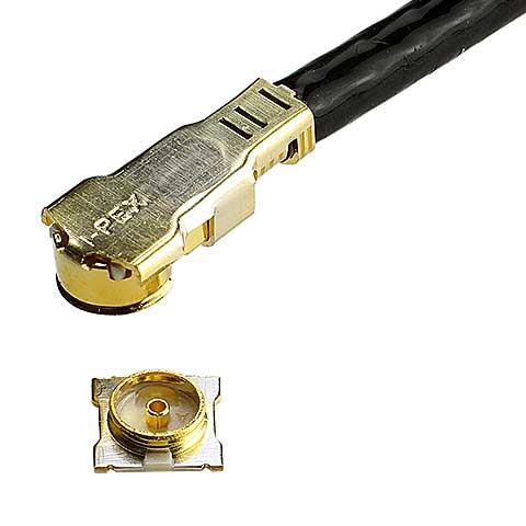
Figure 2 – MHF®7S RF Coaxial Connector |
Category 1 – MHF®7S RF Coaxial Connector The MHF® 7S is a miniaturized connector with a novel stripline launch design. The industry-first connector significantly improves the shielding effectiveness of the coaxial transmission line. Having improved EMI shielding performance, it is ideal for 5G mmWave applications. It has a maximum VSWR of 1.5 at 15 GHz and occupies 2.0 x 2.0 mm worth of PCB real estate. Its mated height is 1.4 mm (max) and it can accept 32 AWG coaxial wire (1.13 mm OD).
|
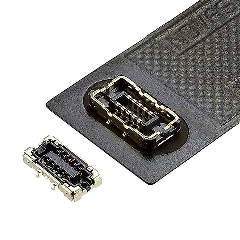
Figure 3 – NOVASTACK®35-HDN Board-to-Board Connector |
Category 2 – NOVASTACK®35-HDN Board-to-Board Connector The NOVASTACK®35-HDN connector was created for 5G mmWave modules. It is fully-shielded, having a 0.35 mm fine pitch and a mated height of 0.7 mm. This connector is ideal for high-frequency applications such as 5G mmWave, Thunderbolt 3, DP, PCI and other high frequency applications up to 15 GHz.
|
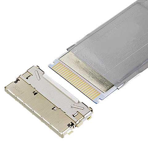
Figure 4 – EVAFLEX®5-HD FFC/FPC Connector |
Category 3 – EVAFLEX®5-HD FFC/FPC Connector The EVAFLEX®5-HD is a 0.5 mm pitch connector with an auto-locking feature. It has horizontal mating and is fully-shielded. Key points Include:
|
ANALYZING EMC PERFORMANCE OF A POTENTIAL CONNECTOR
Radiated Electric Field Emissions
For the FCC (or other EMC regulatory agencies) the topic of electromagnetic compliance necessarily sets and addresses radiated emission limits for the entire computer or device. Since a digital electronic system is composed of numerous components, it stands to reason that a single, unshielded component has the potential to be the weak link that allows EM radiation to propagate in excess of the allowable limits, thereby causing the entire system to fail regulatory EMC testing.
For the purpose of evaluating shielding effectiveness of a component, there are several methods, briefly described below:
- Full-Wave Electromagnetic Simulation is performed using a 3D Field Solver software tool such as the Ansys HFSS (High-Frequency Structure Simulator), CST Micro-Wave Studio, or similar program. In these simulation environments, a 3D mechanical model of the connector pair is imported into the simulator and mounted to a cable, PCB or other transmission line structure in a way that is most representative of its intended use case. Simulation ports are defined at appropriate points in the accompanying transmission line structure or, perhaps, on the input contacts of the connector itself. The output contacts are attached to a short length of transmission line structure (coaxial, PCB, flex circuit, etc.), and terminated in the transmission lines characteristic impedance. The various electrical conditions, such as frequency range, step size, signal amplitude, boundary conditions, and so forth, are then set in 3D solver prior to meshing and iterative solving of the resulting fields associated with the structure. For EMC analysis, radiated E-Field emission is a common metric for analysis of shielding effectiveness.
- An Indoor Shielded Anechoic Chamber, is basically a large metal box with a metal door that properly seals electrically when closed. The room (or chamber) has a non-metallic turntable for positioning the device-under-test, (DUT), a receive antenna and appropriate transmission line fixturing, and is used for the measurement of radiated emissions from the DUT. In the case of a passive DUT, a coaxial input cable is run from a signal source outside the room, through wall-mounted bulk-head coaxial connectors to produce a signal within the DUT. The DUT is then configured with a shielded termination load to eliminate any excess transmission line reflections back through the DUT.
Advantages of this method are that these chambers are commonly in use for measurement of cellular OTA testing (OTA: over the air) and the indoor ranges are usually calibrated for their equivalency to an Open-Air Test Site (OATS). OATS data was originally required by the FCC for Part 15, Sub-Part J compliance purposes.
In this test, the DUT is mounted to the appropriate transmission line, (TL), structure and terminated in the characteristic impedance of the TL. The input line is powered by a signal generator. While signal power is applied to the DUT (at the appropriate frequency), the turntable sweeps the DUT (or the receive antenna). Any emissions are detected by the receive antenna and conveyed to a spectrum analyzer or power meter. This is also commonly done for both shielded and unshielded connectors, to determine the shielding effectiveness of the shielding method employed by the connector.
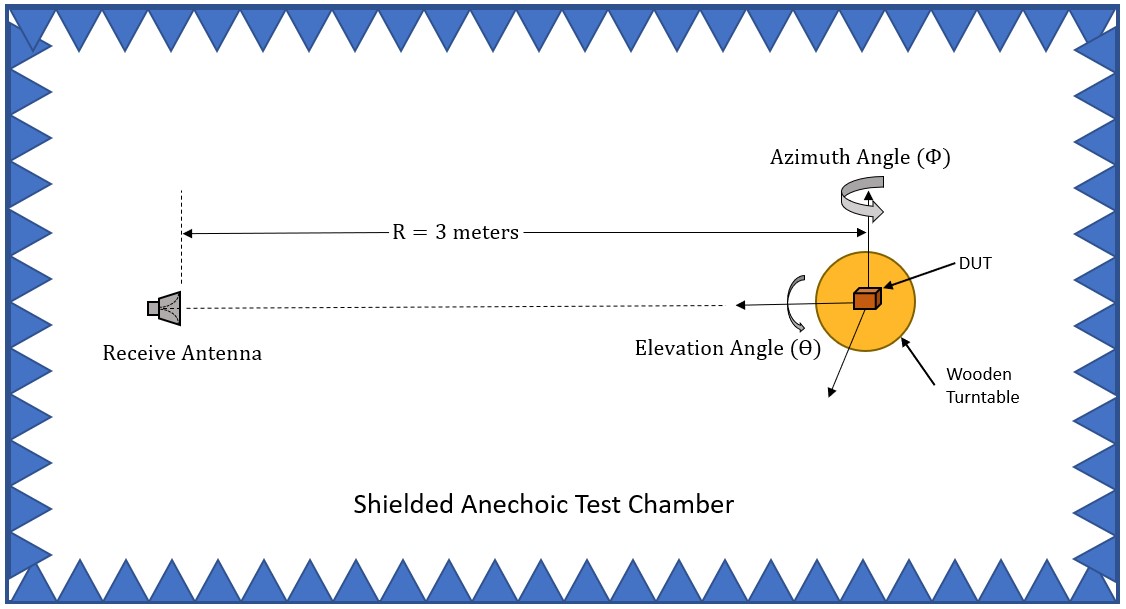
Figure 5 – Antenna Measurement Range Diagram
SECTION 1
HFSS 3D Simulation Results
For the purpose of this paper, and brevity’s sake, full-wave electromagnetic simulation was used to analyze the maximum E-Field leakage of the three prospective connector products. The Ansys HFSS full-wave 3D solver provided the simulation environment by which the connectors were evaluated.
MHF® 7S RF Micro-Coaxial Connector, Low-Profile, Stripline Launch, Locking Connector, HFSS Analysis
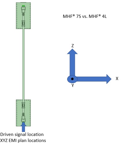
Figure 7 – MHF®7S Driven-Signal Simulation Setup
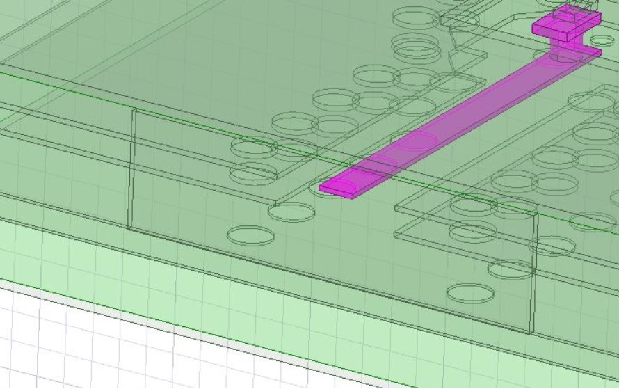
Figure 8 – MHF®7S Port Assignment
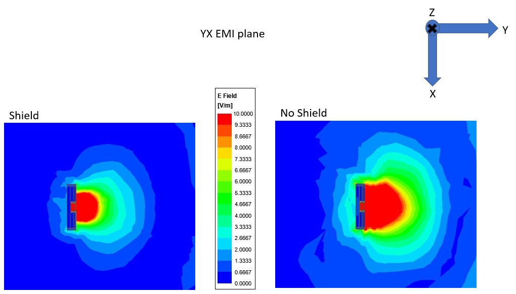
Figure 9 – MHF®7S YX EMI Plane Radiation Pattern
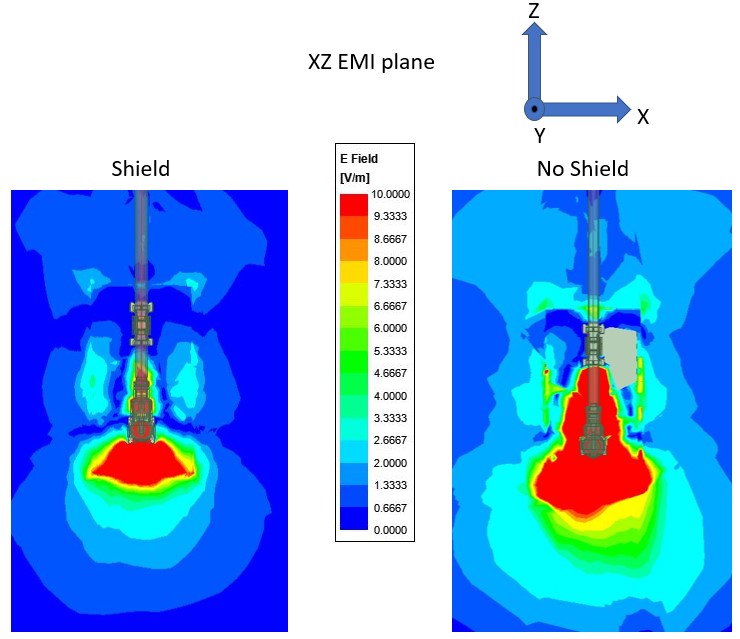
Figure 10 – MHF®7S XZ EMI Plane Radiation Pattern
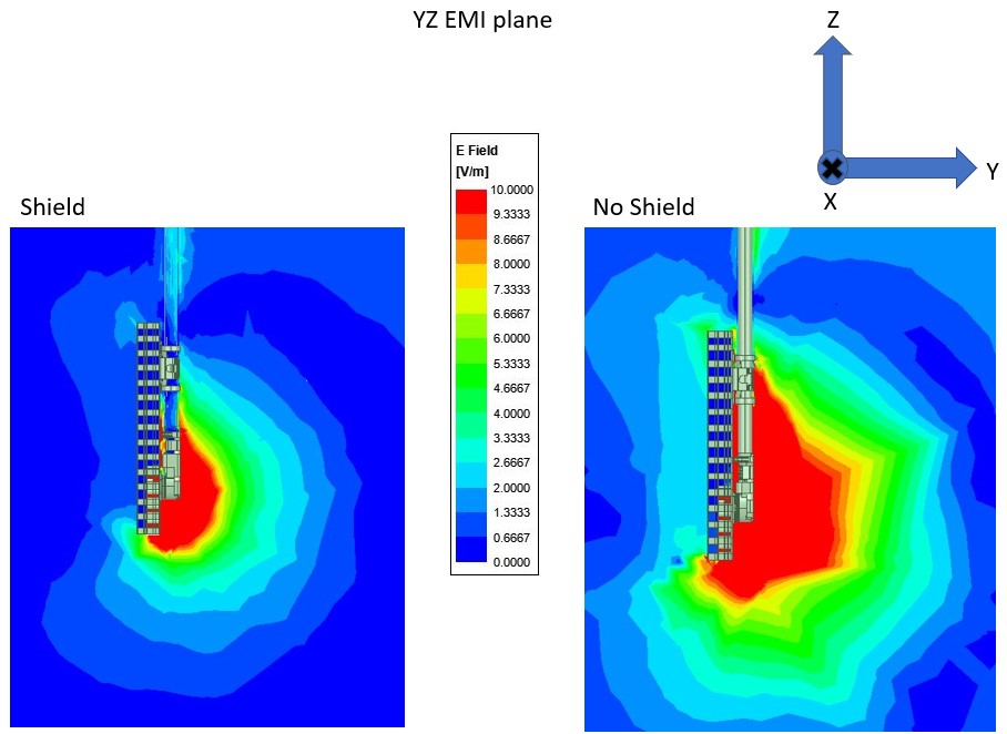
Figure 11 – MHF®7S YZ EMI Plane Radiation Pattern
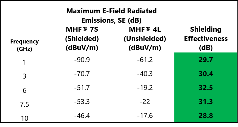
Shielded vs. Unshielded, Radiated Shielding Effectiveness
NOVASTACK®35-HDN Board-to-Board Connector, Ultra-Fine Pitch (0.35 mm) 5G mmWave Connector, HFSS Analysis
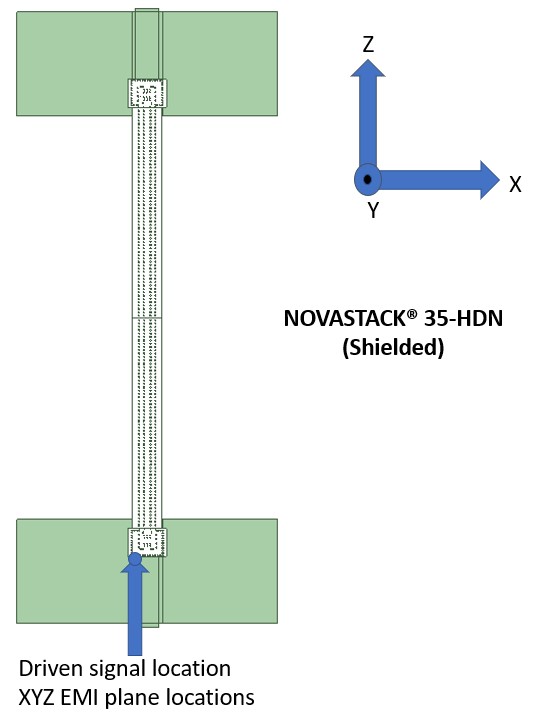
Figure 12 – NOVASTACK®35-HDN Driven-Signal Simulation Setup
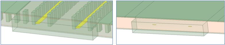
Figure 13 – NOVASTACK® 35-HDN Board-to-Board Connector, Ultra-Fine Pitch for 5G, Port Assignment
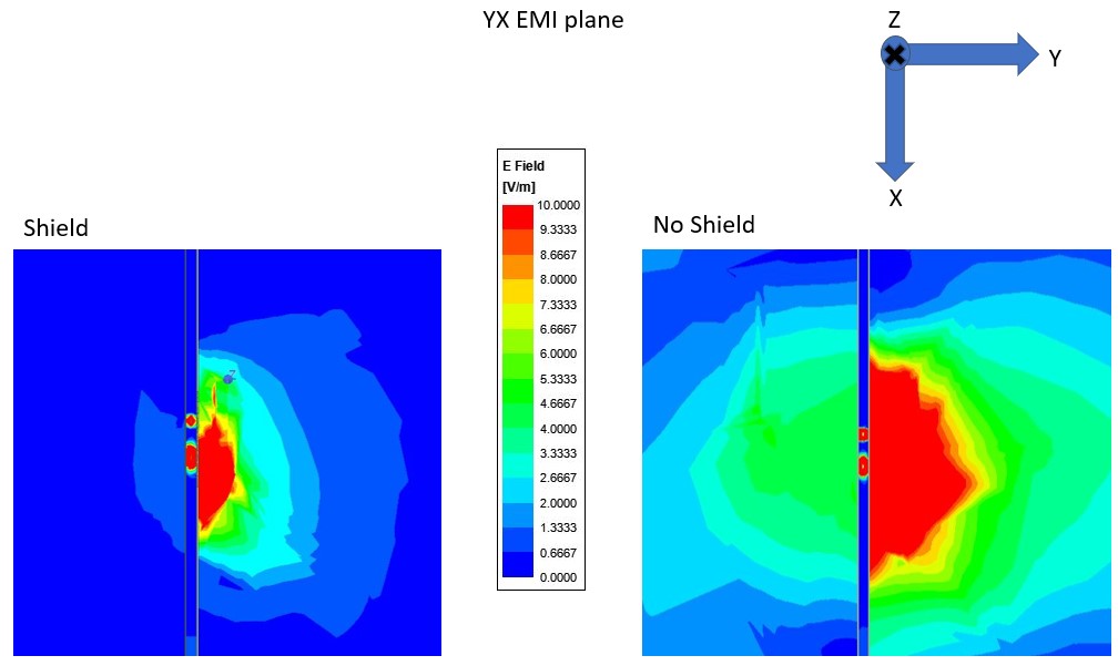
Figure 14 – Ultra-Fine Pitch Connector for 5G YX EMI Plane Radiation Pattern
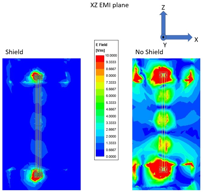
Figure 15 – Ultra-Fine Pitch Connector for 5G, XZ EMI Plane Radiation Pattern
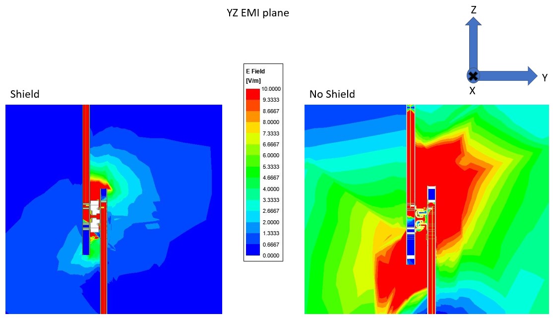
Figure 16 – Ultra-Fine Pitch Connector for 5G, YZ EMI Plane Radiation Pattern
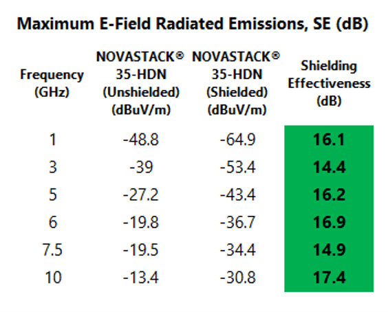
Table 2 – Simulated Shielded vs. Unshielded, Radiated Shielding Effectiveness
EVAFLEX®5-HD FFC/FPC Connector, Flex Circuit, High-Speed, Low-Profile (2 mm height), Fine Pitch (0.5 mm) HFSS Analysis
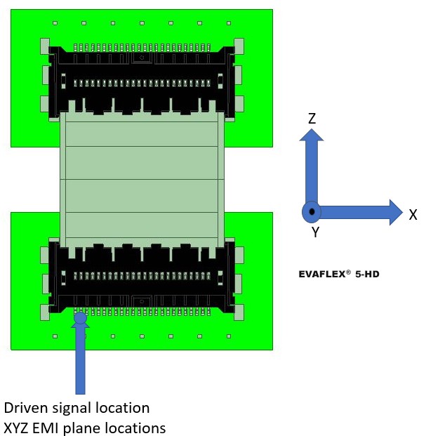
Figure 17 – Flex Circuit Connector, Driven Signal Simulation Set-up
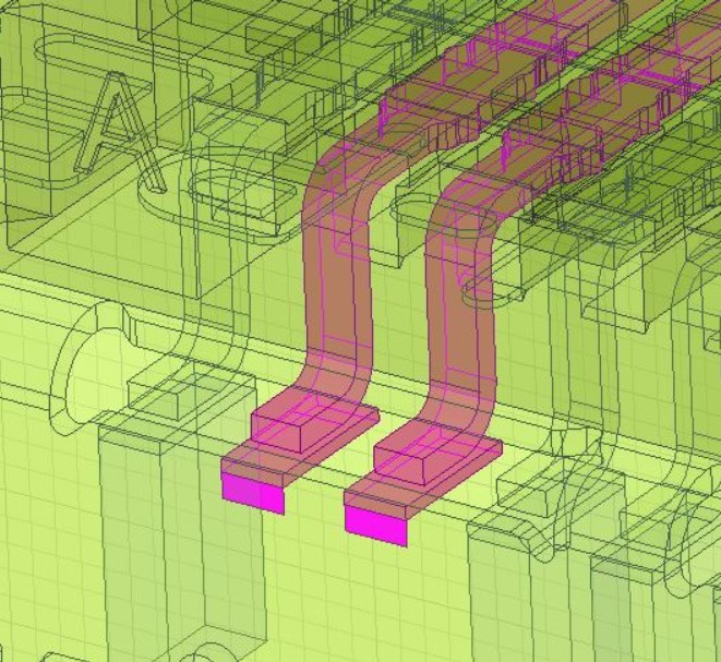
Figure 18 – Flex Circuit Connector, Port Assignment
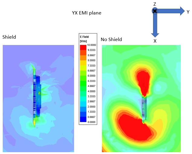
Figure 19 – Flex Circuit Connector, YX EMI Plane Radiation Pattern
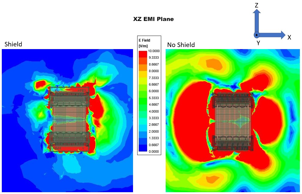
Figure 20 – Flex Circuit Connector, XZ EMI Plane Radiation Pattern
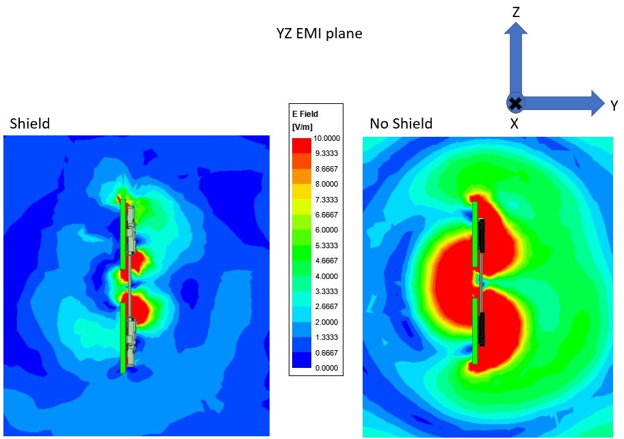
Figure 21 – Flex Circuit Connector, YZ EMI Plane Radiation Pattern
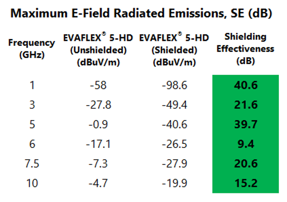
Table 3 – Flex Circuit, Shielded vs. Unshielded, Radiated Shielding Effectiveness
Comparison of Category 1, 2, 3 Connectors
SECTION 2
Maximum E-Field Radiation Leakage Analysis
(Section 1 Results Extended to Component Selection)
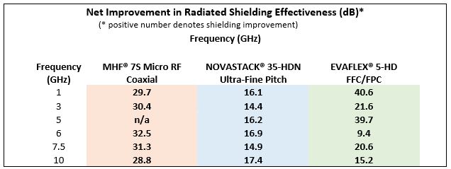
As can be seen from Table 4, all three connector designs' shielding improvements achieved substantial improvements in shielding effectiveness from 1 to 10 GHz. In Section 2, further extension of these maximum Radiated E-Field results will be applied to quantify the maximum input power which can be applied to the candidate interconnect component and still not have the component fail FCC Compliance.
Simplifying assumption. For conservative estimation of maximum allowable power to be applied to the component, there is a substantial simplifying assumption made. This overly conservative assumption is that ALL of the power applied to the connector is available for radiation. In practice, only a small fraction of this “input power” will be potentially radiated. The majority of the power will be passed on along the transmission line to power the intended device load.
How Maximum E-Field Radiation (Emissions from a Shielded Connector) Relates to the Electric Field (Normalized to 3 m) Measured in an FCC OATS or 3m Chamber Compliance Test
To measure maximum electric field radiated emissions, one must employ commonly used antenna characterization methods to determine the radiation pattern from a shielded connector. In actual measurement systems, the radiated emissions from a shielded connector can (and hopefully WILL) be low enough to fall into the background noise level of a routine measurement setup. Decreasing the spectrum analyzer’s resolution bandwidth (RBW), or video bandwidth (VBW), and/or reducing the frequency span, which all require an accompanying increase in sweep time, can lower the noise floor sufficiently to allow detection of a leakage signal from the DUT. This will, however, also greatly increase the overall time for full theta- and phi-angle measurements.
After having obtained the E-Field leakage data, one can easily calculate worst-case E-Field emissions for a given input power to the connector in an actual use case. [Of course, this does not take into account any additional shielding effects contributed by the use of shielded enclosures, gasketing or other EMI mitigation measures.] Refer also, to the simplifying assumption, previously made.
For the purposes of this study, maximum E-Field radiated emissions were obtained by simulation using the ANSYS HFSS Full-Wave Field Solver. Treating the connector (DUT) as an unknown antenna yielded the maximum value for E-Field emissions. Equation 1 shows the relationship between connector maximum radiation (Leakagedut), input power (Pin) to the DUT, and the effective isotropic radiated power (EIRP).
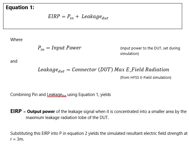
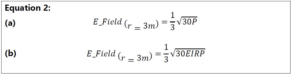
To recap: having simulated the maximum leakage of the interconnect which produced the maximum connector (DUT) leakage, (Leakagedut), this Leakagedut and Pin (set during simulation) were combined using Eq. 1 to give the maximum output power (EIRP) radiated from the DUT. This EIRP was plugged into Eq. 2 to give the expected maximum E-Field at r=3m (for a modeled FCC compliance test result).
But what we wish to know is whether we can determine if a connector, for which we have maximum connector leakage data, can be expected to meet or exceed FCC limits for radiated emissions. To determine this, one can combine Equations (1) and (2b) in order to solve for the maximum input power to the DUT which can still fall within the limits for radiated field strength in the FCC 3m test chamber.

Now by virtue of having simulated maximum E-Field leakage for the prospective ZenShield® Connectors, and equipped with Equation 4, the maximum allowable input power levels by which these DUT’s will still be expected to pass FCC 3m chamber test can be plotted. See graphs 1 and 2 for maximum permissible input power levels in dBm and mW respectively.
Graph 1
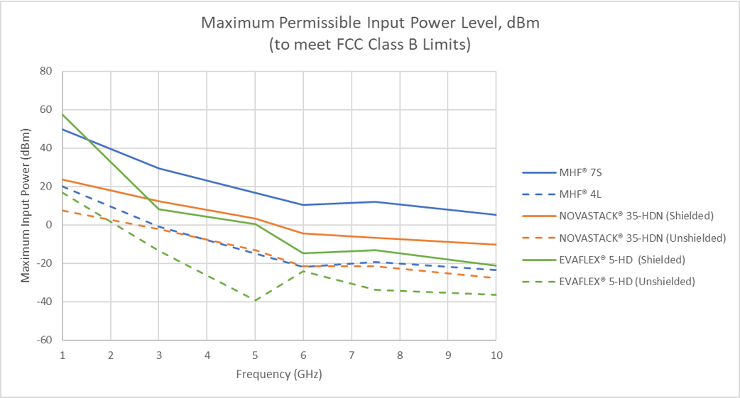
Graph 2
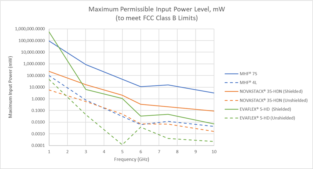
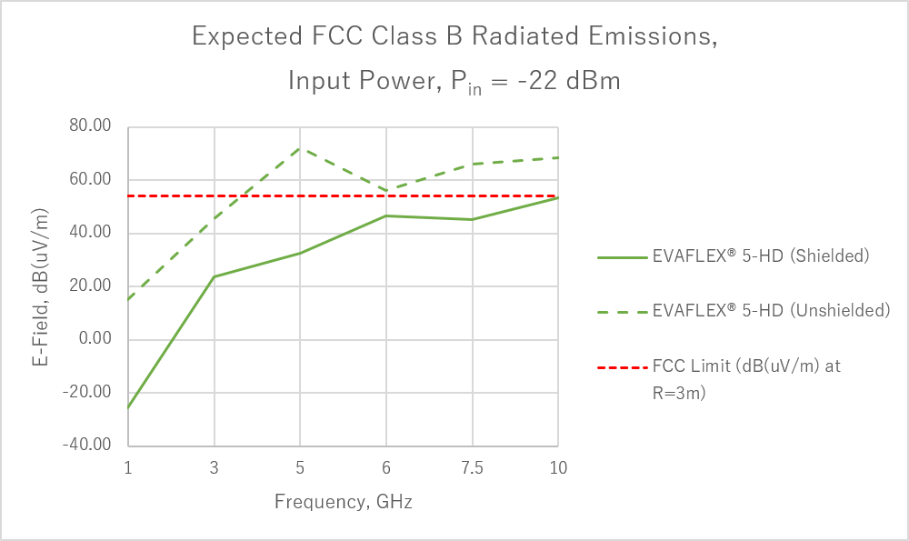
From Graphs 1 and 2, the worst-case (lowest allowable) power levels (usually occurring at 10 GHz), was determined. This is the power level at which a sinusoidal signal at the specified frequency would produce a radiated E-Field (at r=3m) which does not exceed the FCC limits for radiated emissions. For the three shielded ZenShield® Connectors, this maximum permissible power level is listed in Table 5.
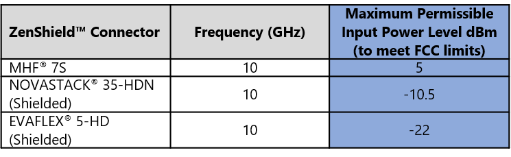
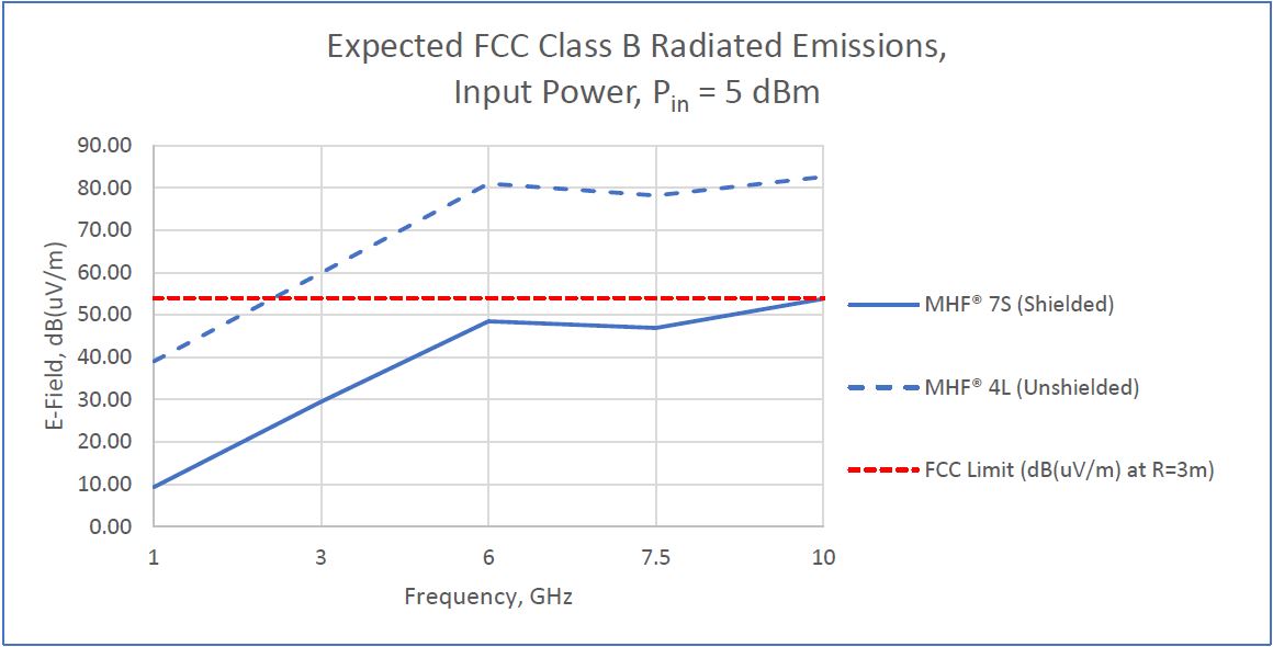
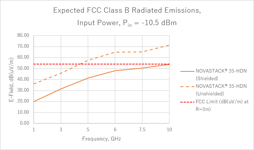
The maximum input power for each DUT was fixed according to the values listed in Table 5. The resulting margin plots were generated in graphs 3, 4 and 5 for the MHF®7S, NOVASTACK®35-HDN and EVAFLEX®5-HD Connectors, shielded/unshielded, respectively.
Graph 3
Graph 4
Graph 5
Conclusion
So, this is interesting data, but one might ask the question, “If we use a ZenShield® Connector, and if the input power is limited to the maximum Pin suggested in graphs 3-5, will our part pass FCC compliance testing?” The answer to this is more nuanced. Since the FCC compliance test is a whole system test, one CANNOT make the general claim that use of a single component will guarantee that the entire system will pass regulatory compliance standards for radiated emissions.
However, one should be able to say that IF their system FAILS the FCC compliance testing, and IF the internal power levels did not exceed those that were used in this simulation (Po <= Pmax), THEN the system should NOT FAIL as a result of using this particular ZenShield® component. We believe that this design guide is a useful starting point to assist the designer in selection of mmWave or Multi-Gigabit interconnect component selection.
For physically small spaces, high-volume, high-frequency applications, where cost, space, bandwidth, performance and radiation limits must all be observed, the ZenShield® family of connectors will likely have a solution that is a great fit for your application.