PCB Stack Up Optimization Services
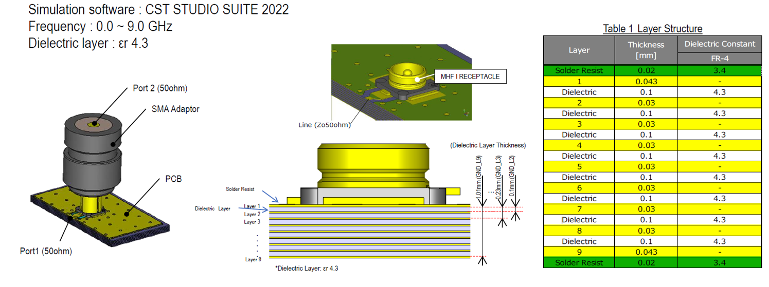
PCB lay out, choice of materials and stack up of Signals and GND layers plays a crucial role in optimal signal integrity of MHF® series connectors. GND cut out sections under the MHF® receptacles ensure low Return Loss and VSWR across the entire operating frequency range. I-PEX recommends a PCB lay out as shown in Figure 1 below for optimal signal integrity performance as a reference. Please note that resulting S Parameters from your board design may vary with different materials or layer thickness. If the simulation with your designated Board is needed, please provide your board lay out including material selections and layer stack up and geometry and we can help simulate the expected S parametric performance for optimizations.
Figures 2 and 3 show the recommended GND cut out areas under the MHF® I receptacle mounted on PCB. Figure 4 shows the recommended board side soldering footprint for connector.
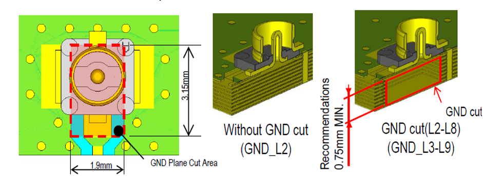
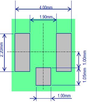
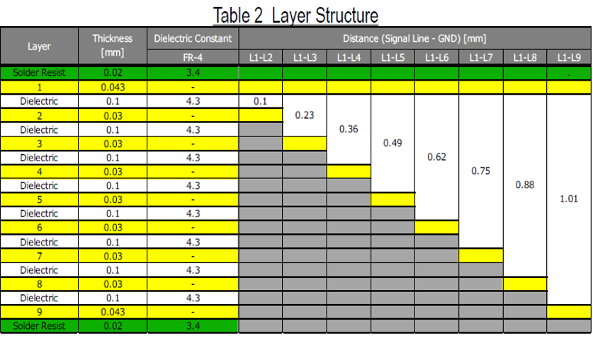
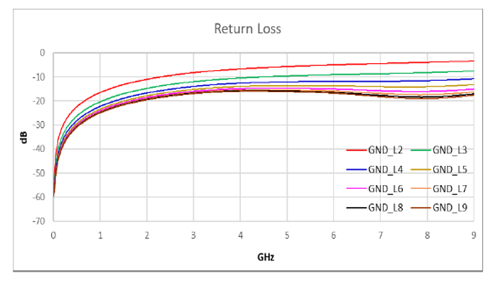
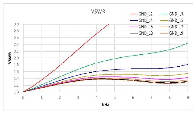
Table 2 shows the variation in distance between the Signal and GND layers of PCB for MHF® I receptacle. Graphs 1 and 2 show the resulting variation in Return Loss and VSWR performance of MHF® I connector.
Based on the simulations, it can be concluded that S parameters with the cutout on layer 7 or lower layers are almost same. Based on this result, we recommend securing the space of 0.75 mm or greater depth between the receptacle SMT layer and the ground layer under the receptacle.
Features and Benefits of I-PEX RF Solutions
- 1. Compact Size and High Density
- 2. High Frequency and Data Rates
- 3. Superior EMC Performance
- 4. High Design Flexibility
- 5. Robust Design with Integrated Locking Features
- 6. Key Industry Standards
- 7. Consistent Performance with i-Fit® Technology
- 8. MHF® Switch Products for Antenna Testing
- 9. Available Accessories
- 10. PCB Stack Up Optimization Services