4K2K Display Graphics Connector – Mitigating EMI
Contents :
Solder Tail Shielding Mitigates EMI
Balanced Grounding at the Termination
Shielding the Termination
Impedance Continuity of the Graphics Connector
Insertion Loss and Return Loss (s12p)
Introduction – Solder Tail Shielding Mitigates EMI
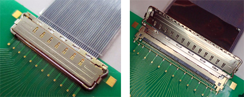
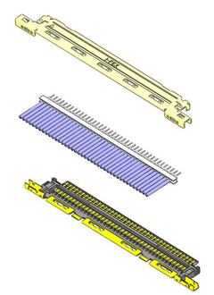
The display graphics connector’s exposed solder tails transfer 5.4 Gbps, radiating EMI at a Nyquist frequency of 2.7 GHz, which interferes with many wireless carrier frequency bands. They need to be shielded. No longer will device solutions require a secondary value-added action (i.e. applying metallized tape or an extra metal cover to be added over the graphics connector) since an integrated solder tail shielding feature shown in Figure 1 has been designed into the display graphics connector.
Balanced Grounding at the Termination
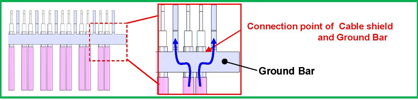
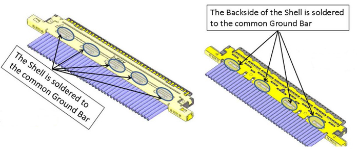
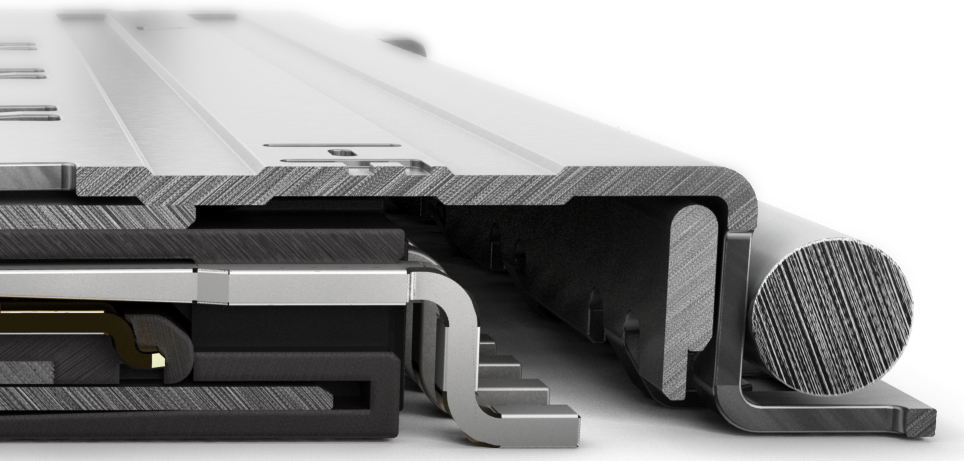
The differentially driven coaxial wire termination in the high-speed graphics connectors is an internal Faraday-caged wire termination area. The prepared coaxial wire assembly has exposed shields that are soldered to formed grounding bars on the top and bottom creating a solid grounding bar construction by completely filling each fillet (void) between the coaxial wires as shown in Figure 2. This also provides a mechanical strain relief for the center conductor attachment to the connector plug housing with when someone pulls on the cable’s wires.
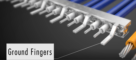
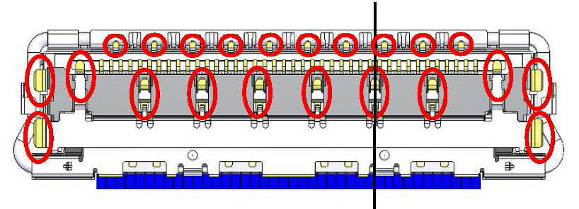
Ground fingers provide a shroud between each differentially driven coaxial wire pair. This provides the shortest high-speed path to ground shown by the blue arrows in Figure 3 below.
The grounding fingers provide a differentially driven coaxial transmission line with the balanced termination needed for acceptable high-speed differential data like the signals shown in Figure 4.
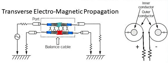
An “unbalanced” termination can generate a large amount of differential to common mode conversion (Scd21 – noise - known as Transverse Conversion Transfer Loss) and EMI. Figure 5 shows a balanced termination - the positive capacitance cancels the negative capacitance. Good ground bar construction typically results in the Scd21 performance of the termination at about-25dB.
Shielding the Termination
After the prepared wire assembly is attached to the plug housing, a top metal shell is then applied over the area where the coaxial wires are terminated.
The shell is then soldered to the grounding bar both on the top and bottom of the plug connector assembly.
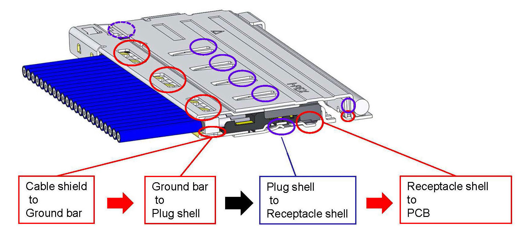
The shield grounding path goes through the connector’s shells from the coaxial wire shields which are attached to the ground bar which is attached to the plug shell. The plug shell engages with the receptacle shell as shown in Figure 8, which takes the shortest path to ground along the span of the receptacle bottom contacts shown in Figure 9. The short ground paths enable good high-speed signal transfer performance.
Clearance between the shielding lid/bar and the solder tails was considered as a possible area where shorting could occur. This design (Figure 10) ensures an absolute clearance minimum of 1.7 mm.
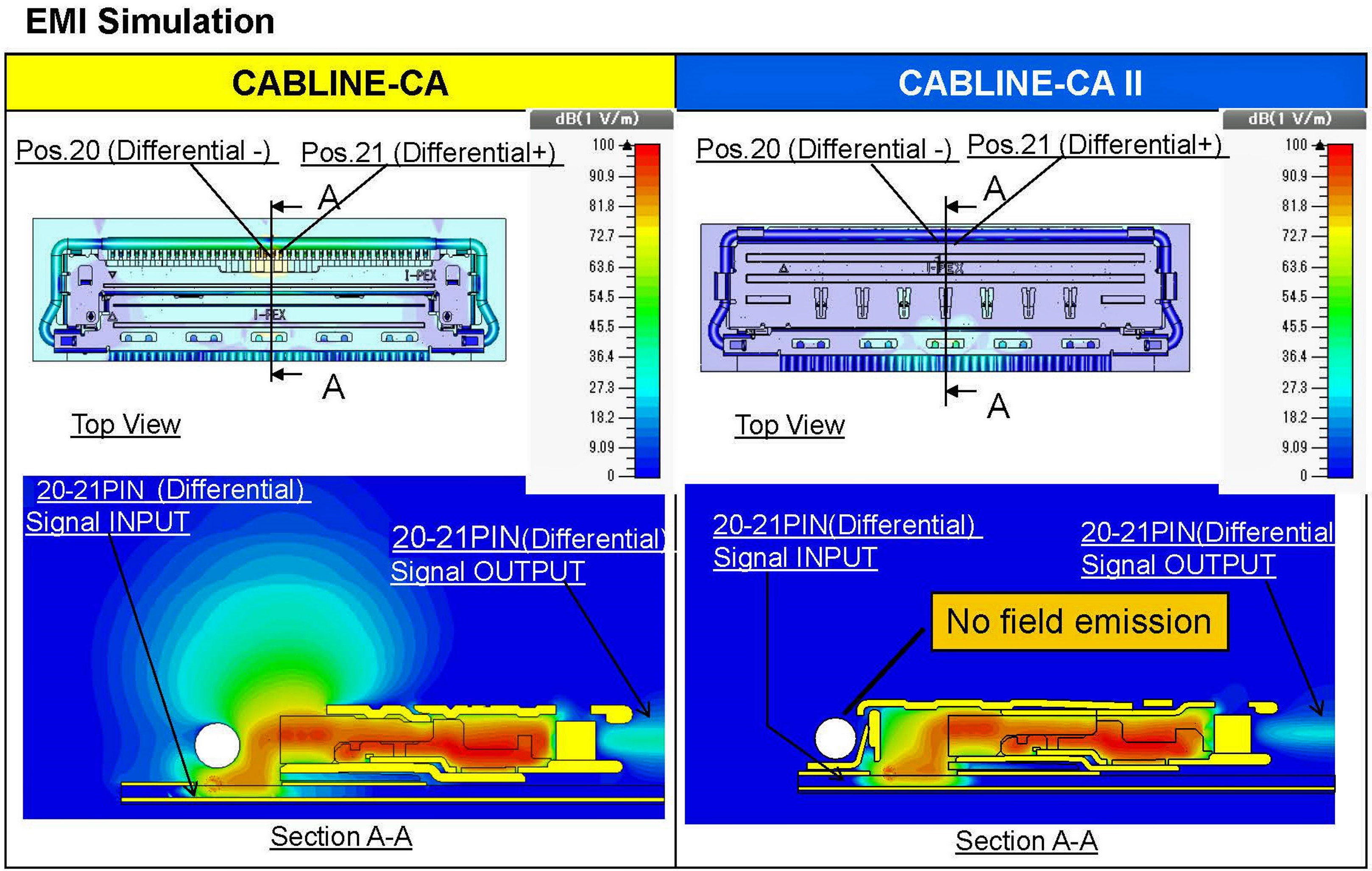
Using CST Microwave Studio as shown in Figure 11, an electric field strength analysis was performed to compare the graphics connector’s radiation with and without the solder tail shielding.
The 3-lane simulation was performed near one side at the locations of Pins 2 and 3, and also near the middle of the connector at Pins 20 and 21. A third location was analyzed between the shield cover ground spring fingers near Pins 8 and 9. The setup conditions for the simulation are shown in Figure 11 using the GSSGSSGSS signal assignment pattern.
A comparison of the E-fields strength when transferring a stressful 20 GHz signal through the graphics connector with the solder-tails covered by the shielding lid and without the solder-tails shielded is shown in Figure 12.
The E-Field simulation for the three locations Positons 20-21, 2-3 and between the ground springs for the connector are shown in Figure 13 at 2.4 GHz frequency (~5 Gbps) and Figure 14 at 5 GHz (~10 Gbps).
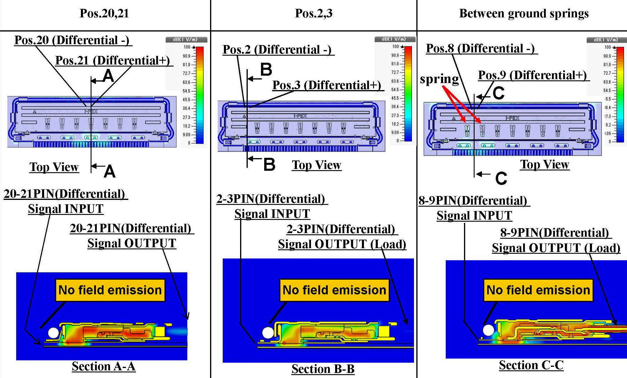
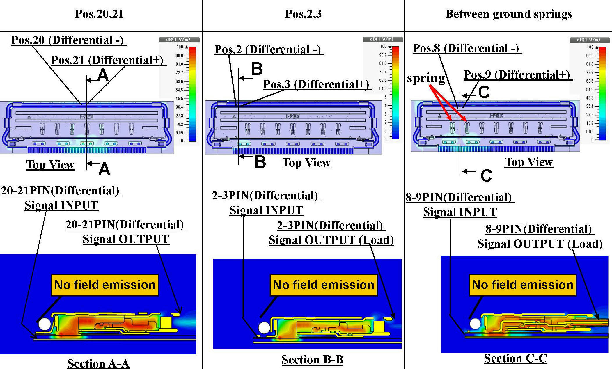
The simulation shows that no E-fields radiated from the graphics connector when the solder-tails are covered by the shielding lid. Data rates are related to frequency by the term “Nyquist frequency.” The HBR2 5.4 Gbps Nyquist is 2.7 GHz which is the same frequency as some LTE carrier bands. When located in close proximity to the LTE radio/antenna ~2.7 GHz carrier signal, the unshielded solder tails of the graphics connector radiates a Nyquist frequency of ~2.7 GHz. Interference between Nyquist frequency radiation from the connector solder tails and the LTE wireless radio/antenna carrier frequency ~2.7 GHz causes the communications links to fail.
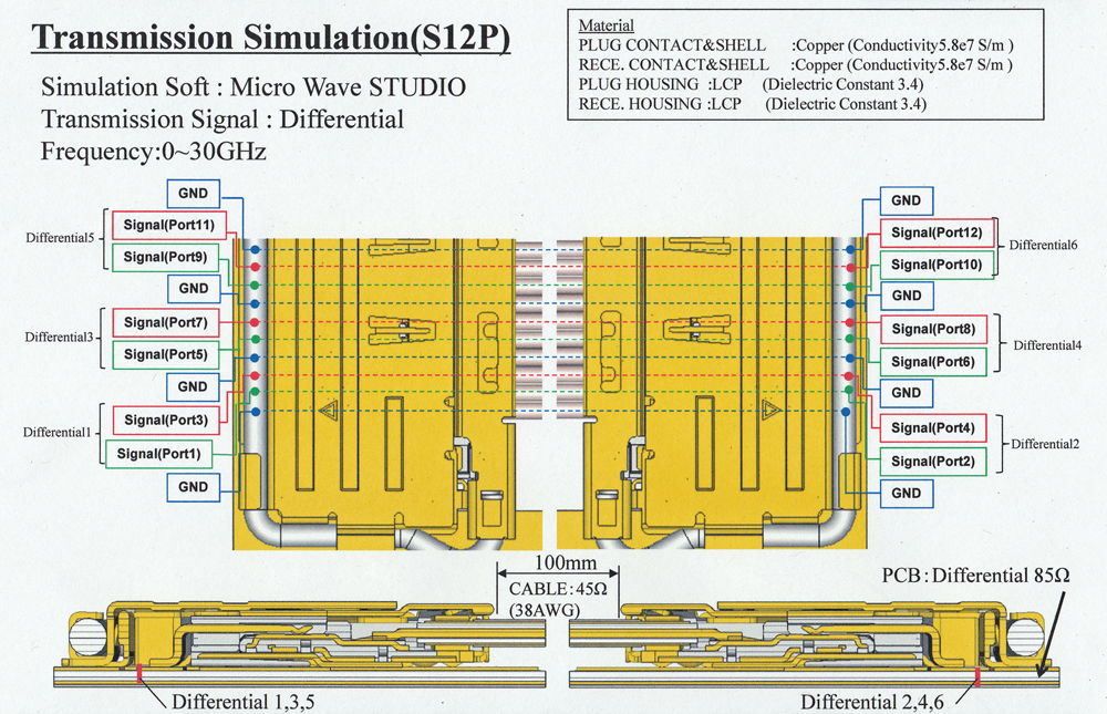
The EMI concerns are solved. The signal integrity performance analysis can now be addressed. The characteristic impedance profile as analyzed in the time domain and scattering parameters (S-parameters) are used for analysis of such parameters as Insertion Loss, Return Loss, Far End Crosstalk, Near End Crosstalk, and as previously discussed the Differential to Common Mode Conversion (Scd21) all in the frequency domain. A 3-differential lane analysis as shown in Figure 11 produces a s12p file that can be shared by Touchstone format.
Impedance Continuity of the Graphics Connector
The superior ground structure of the graphics connector enables the eDP HBR2 5.4 Gbps differential signals to transfer through the connector with a very small amount of impedance discontinuity. Typically the 5.4 Gbps data rate would equate with a rise time of Tr=64ps (20%-80%) but since Tr=40p (20%-80%) is suggested by USB-IF for the 10 Gbps data rate the performance analysis used Tr=40ps (20%-80%) as shown in Figure 15.
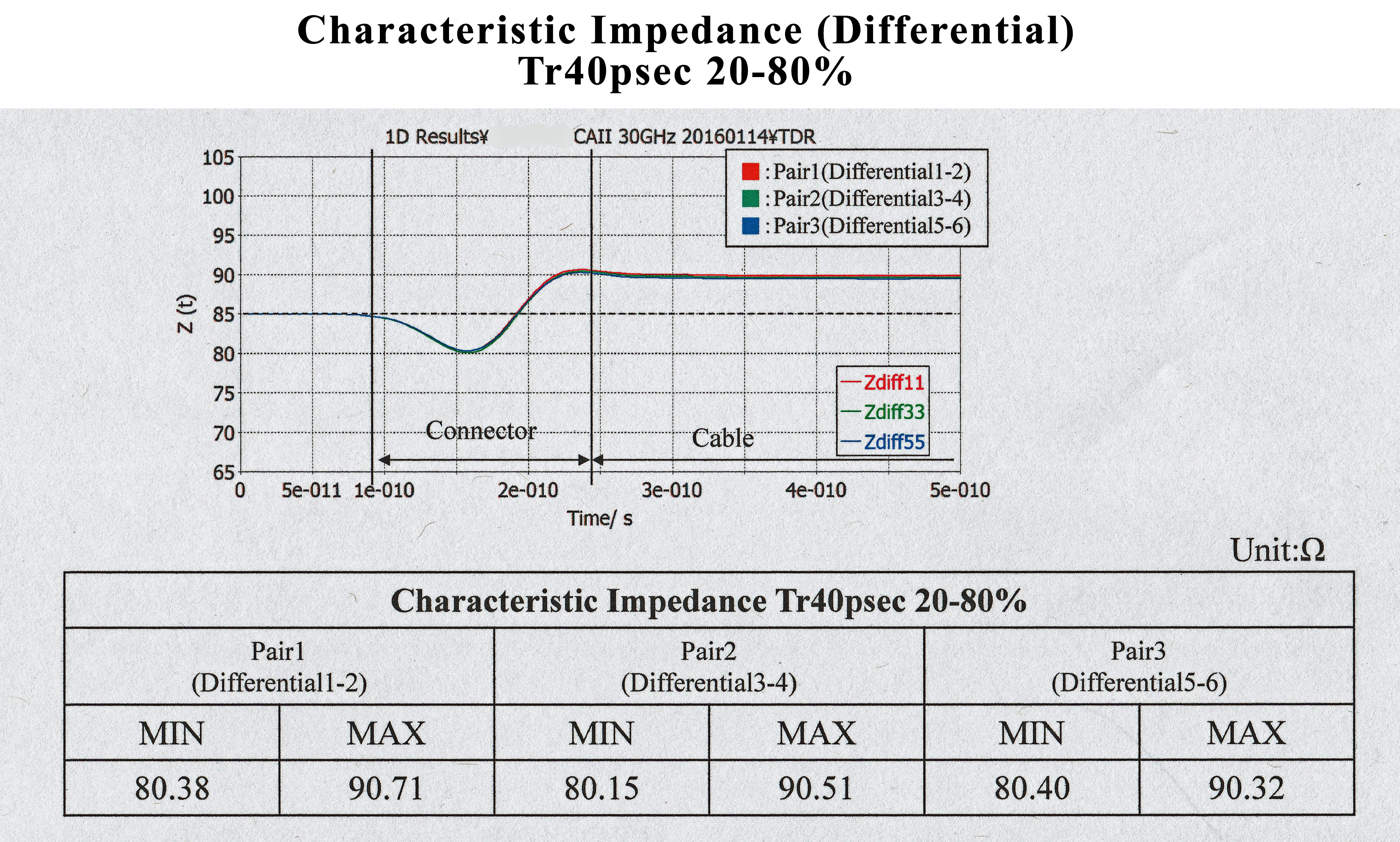
The average impedance discontinuity through the connector at 10 Gbps (5 GHz) is ~Δ10.2 ohms. This result indicates that the connector should have good return loss (low reflections) and good crosstalk (high isolation) performance. A transmission channel that has large impedance path variations (discontinuities) exhibits poor return loss and crosstalk. Differential to common mode conversion is also expected to be worse.
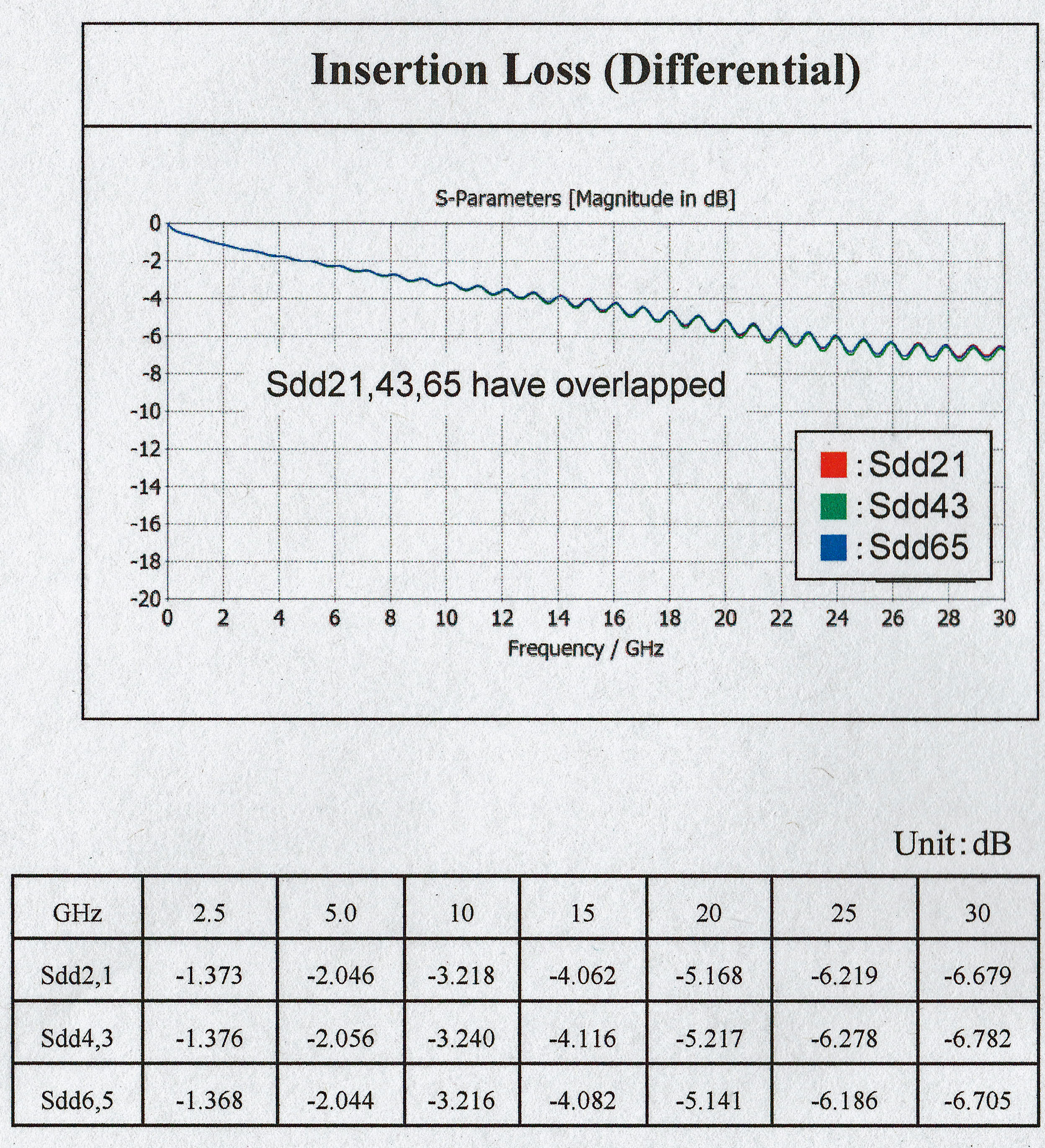
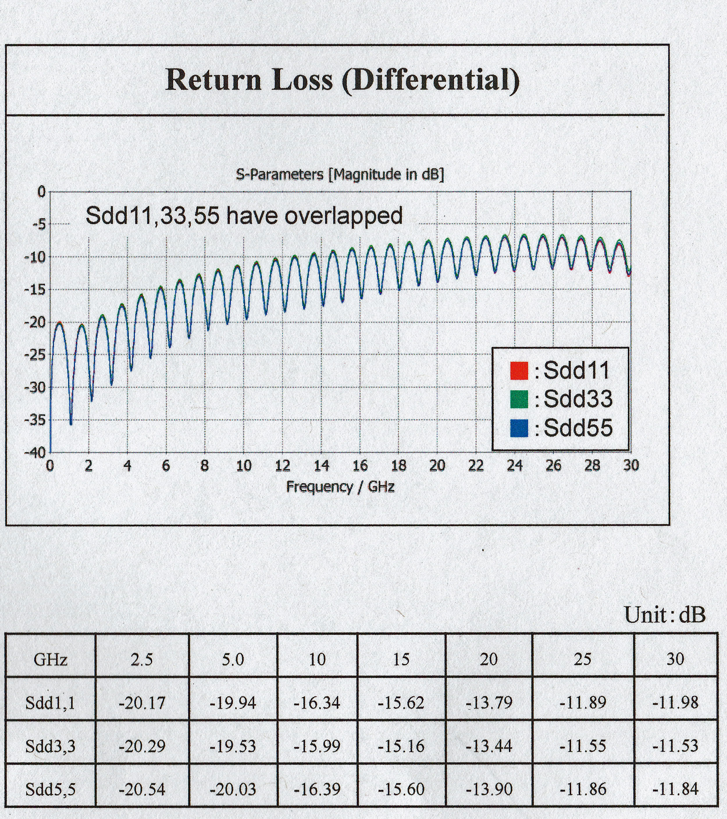
Insertion Loss and Return Loss (s12p)
The insertion loss for a 100 mm long terminated cable using microcoaxial wire AWG38 with 45ohm controlled impedance is shown in Figure 16. For example, at 5 Gbps (2.5 GHz) the IL is < 2dB.
The return loss for the 100 mm long cable shown in Figure 17 becomes unacceptable when it gets worse than -10dB (above 12GHz). The shorter the cable the worse the return loss since the return path for the reflection is shorter.
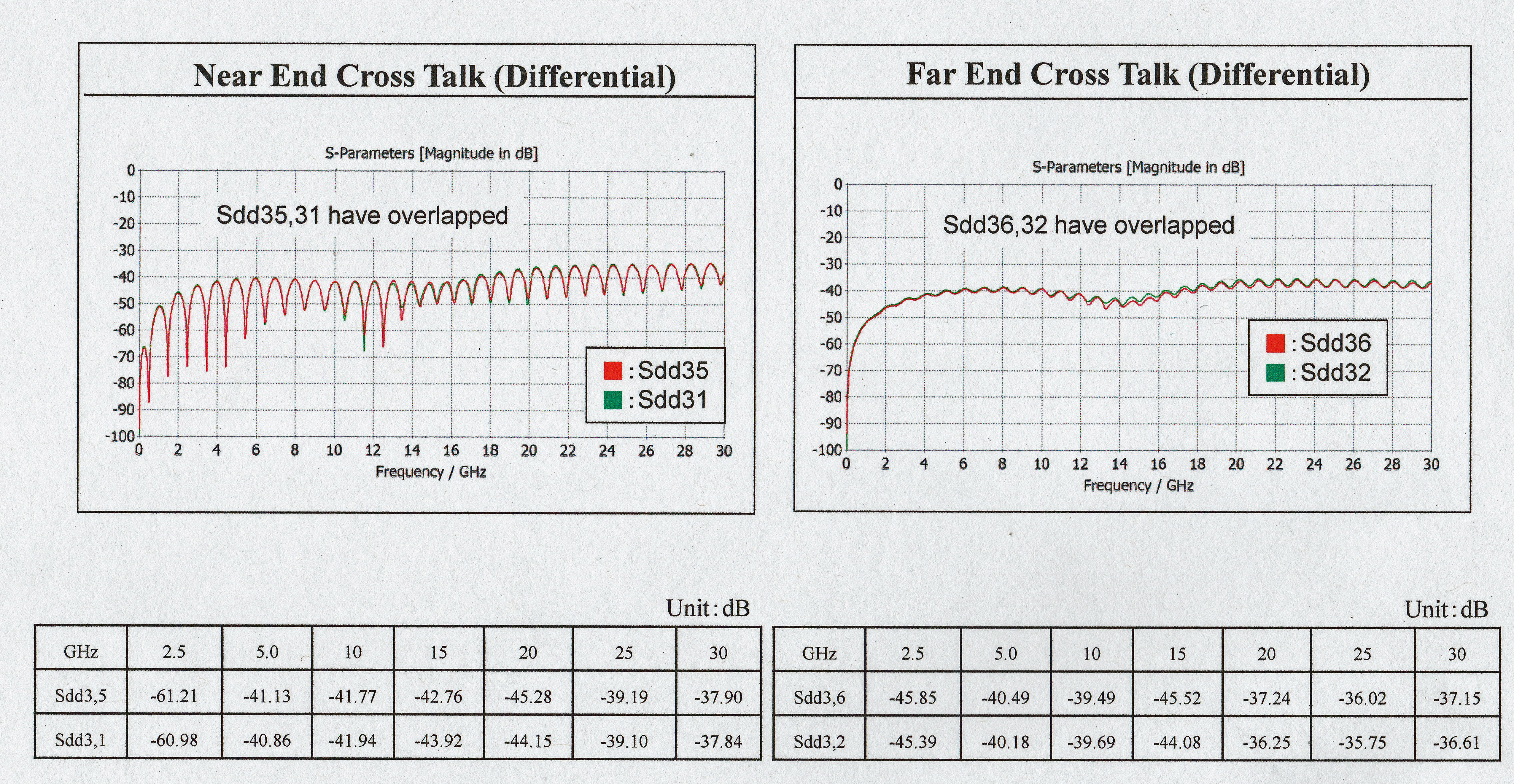
The simulated crosstalk performance for the cable shown in Figure 18 also appears to have good results.
The eDP graphics connector design with an integrated locking shielding lid has the feature set to support the higher resolution display assemblies as the data rate continues to accelerate.
References
1. I-PEX, “IER-001-07244-00,” Simulation Transmission, January 15, 2016
2. I-PEX, “IER-001-06877-00,” Grounding Bar Design, May 29, 2015
3. David E. Bockelman and William R. Eisenstadt, “Combined Differential and Common-Mode Scattering Parameters” IEEE
Vol.43, No.7, July 1955