High Data Rates
Data rates play a critical role in today's smaller and faster electronic systems. It is important to maintain the high data rate for signals going between multiple printed circuit boards, when stacked in high density, compact devices for optimal performance. Data rates are typically determined by maximum operating frequency and are specified in Gbps. NOVASTACK® series of products can support maximum frequency of 20 GHz and data rates up to 80 Gbps using PAM4 signalling. USB, MIPI, LVDS, eDP, Thunderbolt and PCIe are some of the commonly supported proctocols by NOVASTACK® series products.
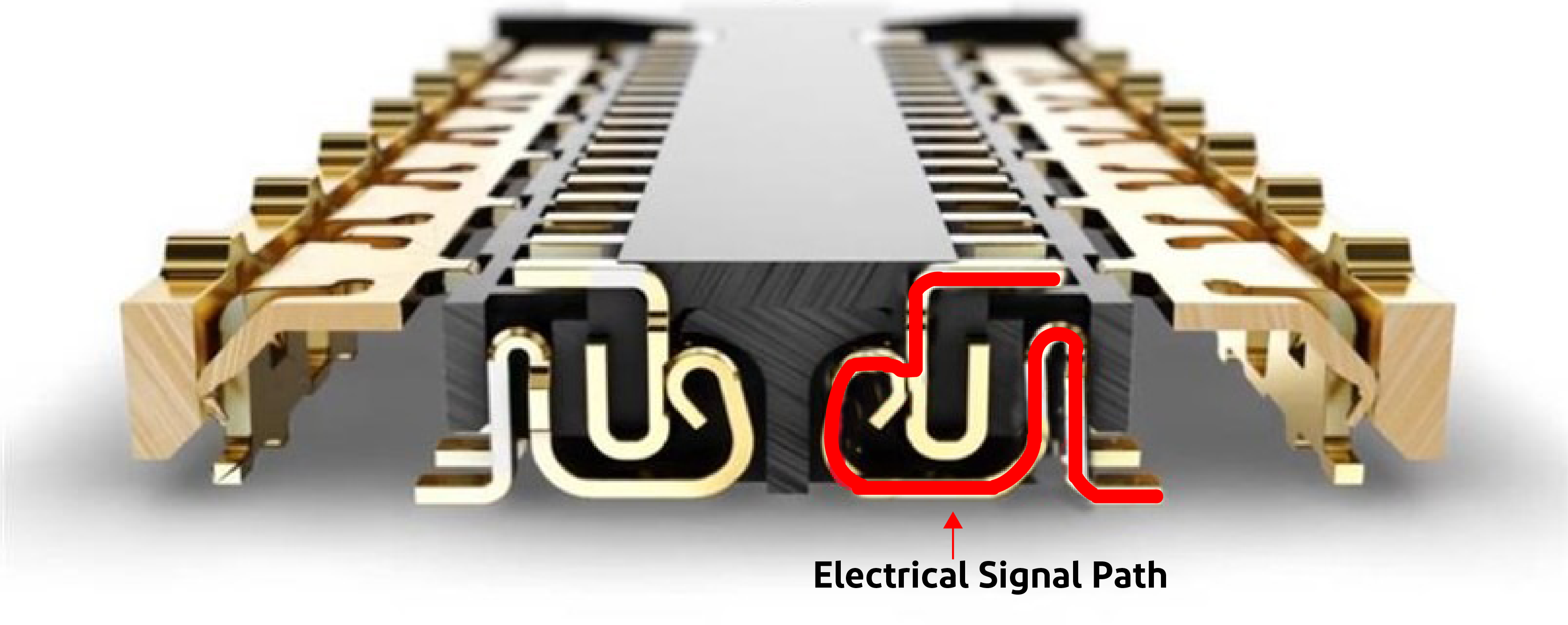
High definition displays, faster processing speeds of smaller servers and personal computers, higher resolutions of medical imaging systems and use of 3d graphics in Augmented, Virtual and Mixed Reality headsets are driving the faster data rates for PCBs. With data rates in the range of 20 Gbps+, it becomes quite challenging to maintain the signal integrity of signals and the design of board to board connector plays a vital role in over all system performance. Insertion Loss, VSWR, Near End and Far End Cross Talk are some of the key Signal Integrity Indicators for these connectors. Insertion Loss can be simply put as the amount of high frequency signal lost as heat with in the contacts of connector. Shape of contacts and total length of signal path in mated contact pairs determines how much is the insertion loss of signal in connector only. A longer signal path typically results in higher insertion loss, resulting in lower effective data rates. Figure 1 shows the structure of NOVASTACK® series connectors including the mating length of the contacts.
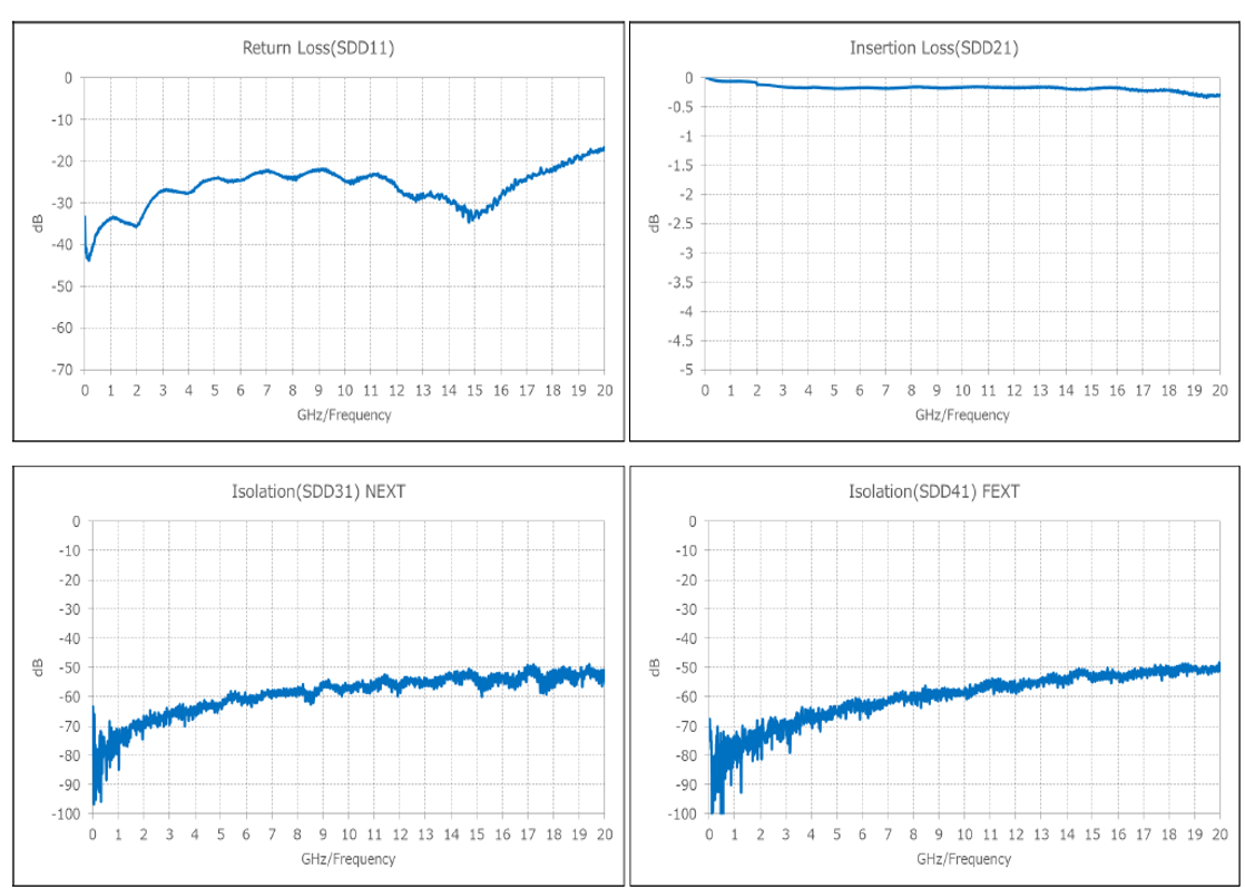
Return Loss is the signal loss due to reflections from either transmitting and receiving side of connector. These reflections are caused by the impedance mismatch of all the components of high speed channel including the contacts in connector itself. Like Insertion Loss, Return Loss also increases typically with the higher frequencies and a good design of connector plays an important role to keep it low.
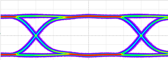
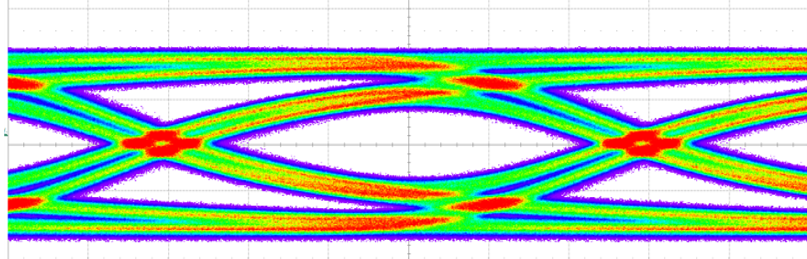
Impedance matching of signal contacts in connector ensures the signals are transmitted or received fully by the connector. With the mismatch in contact impedance, signal reflections are introduced fromtransmitter and receiver side contact resulting in Standing Waves along the channel, a phenomonan commonly known as VSWR. A high VSWR value results in signal loss. Impedance mismatch and high losses result in closed Signal Eye in high speed signal transmission leading to high Bit Error Rate and data loss on receiving end. For this reason, it becomes even more important to use a high performance, low loss board to board connector with well matched impedance.
There is mutual coupling of high speed signals in an interconnect medium like connectors. Due to this coupling, often times, some of the signal appears as unwanted noise on the unused contact. This unwanted signal noise is called Cross Talk and is measured in decibels, dB. When the cross talk noise appears on the contact adjacent to the driver contact, it is called Near End Cross Talk or NEXT and when the cross talk noise appears on the ununsed contact on the farther end, it is called Far End Cross Talk or FEXT as shown in the pin assignment of Figure 3 below. Typically, the cross talk increases with the increase in signal frequency.
Since it is measured on negative scale as noise, a higher value means lower cross talk. For example, a cross talk (NEXT) of -55 dB at 10GHz is lower than NEXT of -50 dB at 20 Ghz in the plots shown in Figure 3 below. Cross talk noise also depends on the pin assignment for high speed signals and ground pins in connector. Crosstalk data shown in graphs below is assuming a pin out shown in image next to the graphs below. The inclusion of multiple GND pins between high speed differential signals helps to reduce the coupling of signals from agressor/ active channels to victim/idle channels and minimizes the overall cross talk. Also, the Return Loss and Insertion Loss data is also shown in the same plots in Figure 3 for NOVASTACK® 35-HDH connectors.
| Plug | 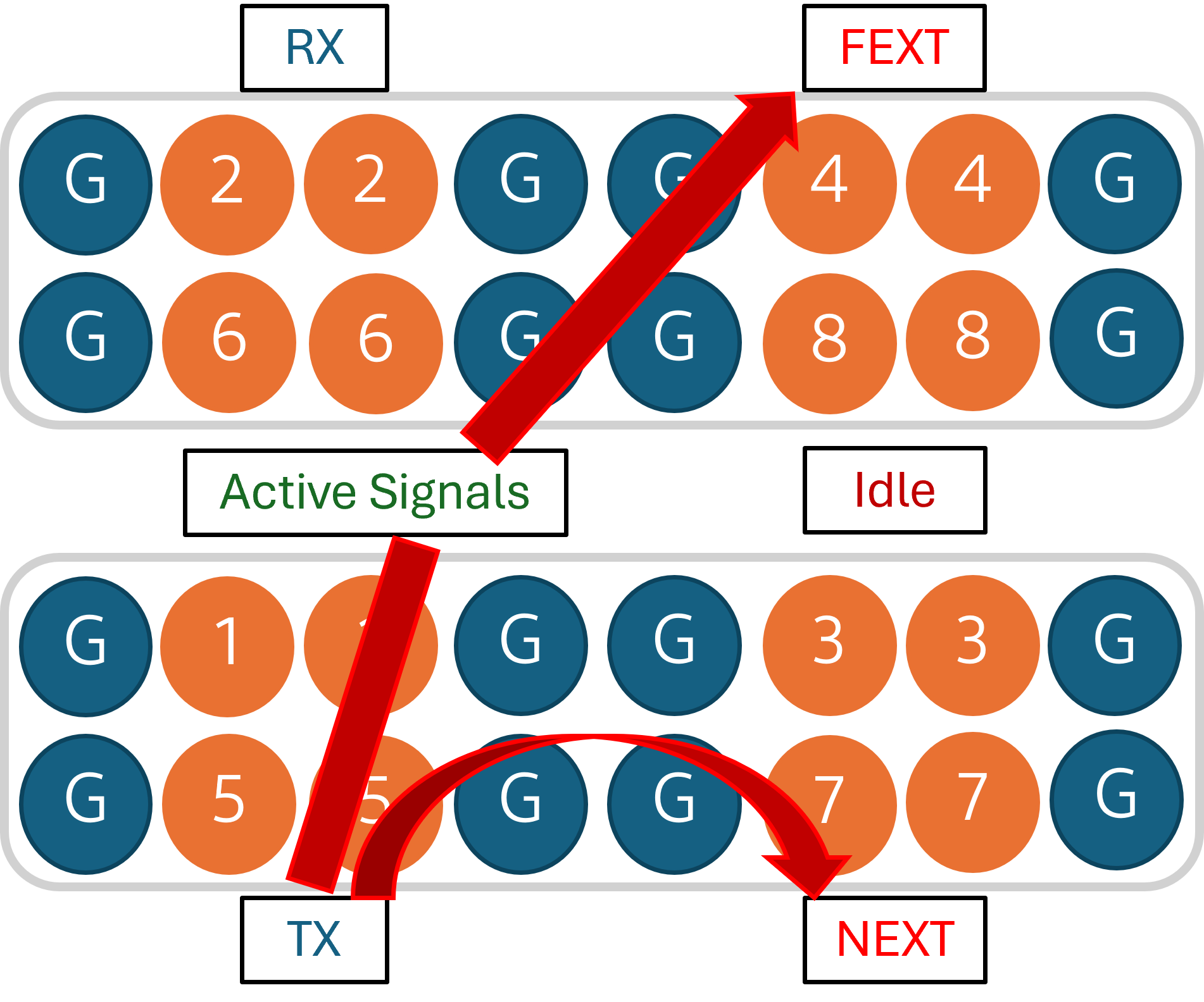
|
| Receptacle |
I-PEX offers Signal Integrity Test Boards for both receptacles and plugs of NOVASTACK® series connectors.
Learn More about SI Tools