Wafer Products (KRYSTAL® Wafer)

KRYSTAL® Wafer
Superior wafers for piezoelectric MEMS, that can be single-crystallize various piezoelectric materials to be deposited by using our original ZrO2 Buffer.
- Standard PZT KRYSTAL® Wafers
- Multi-layer Single-Crystal PZT (2-layer) Wafer
- Aluminum Nitride (AlN) Thin Film Wafer
Standard PZT KRYSTAL® Wafers

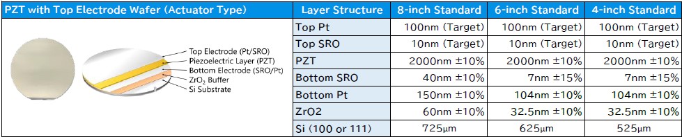
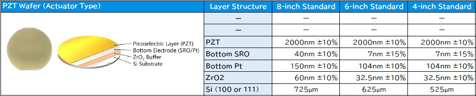
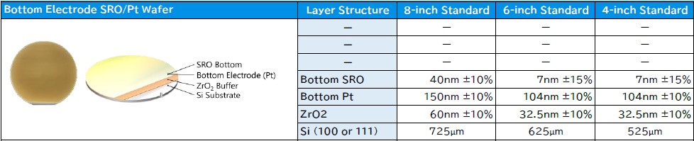
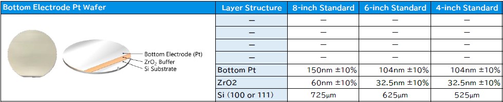
- Standard wafer sizes: 4-inch, 6-inch, and 8-inch sizes
Single-Crystal PZT with Top Electrode Wafer
Single-Crystal PZT Wafer
Bottom Electrode SRO/Pt Wafer (SRO/Pt/ZrO2)
Bottom Electrode Pt Wafer (Pt/ZrO2)
ZrO2 Buffer Wafer (ZrO2)
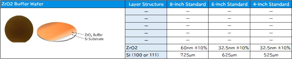
In addition to standard deposition on Si wafers, we also provide custom deposition services, such as deposition at different thicknesses, deposition on SOI wafers, and deposition on wafers supplied by customer.
New Technology Developments
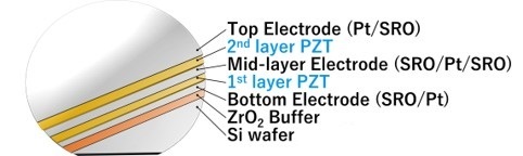 Multiple layers of single-crystal PZT are deposited by applying superior deposition technology. Piezoelectric properties are improved, enabling high-power and high-precision actuator drive.
Learn More
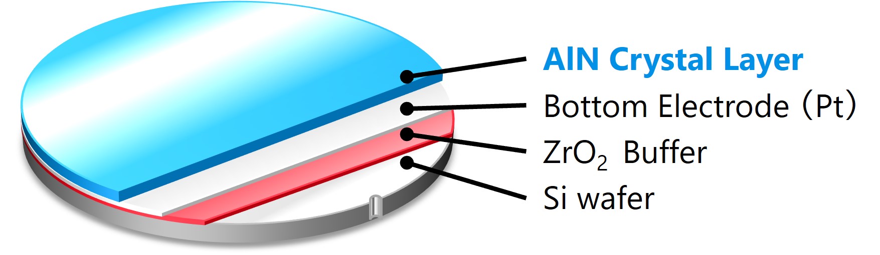 Achieved AlN epitaxial growth on Si wafer using our unique ZrO2 buffer layer technology.
Learn More