FAQ
Frequently Asked Questions (FAQ)
About MEMS Processing Service
- Is it possible to request only specific MEMS processing?
- Is it possible to request processing of the supplied PZT wafers made by other companies?
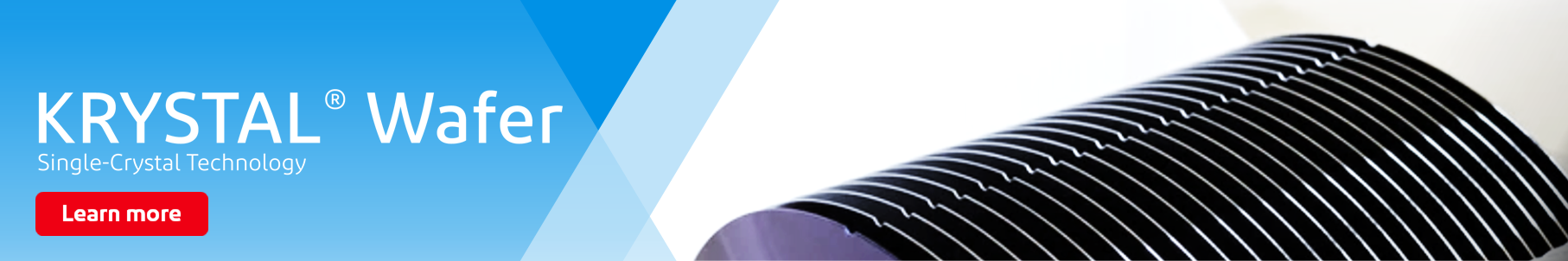
About KRYSTAL® Wafer Products and Deposition Services
- What types of unique features does single crystal PZT have?
- It seems that KRYSTAL Wafer has single crystal PZT for sensor applications and for actuator applications, but how do they differ?
- Can you deposit films on any wafers?
- We would like to purchase Bottom Electrode Type Krystal Wafers, and make our own single-crystal piezoelectric film, will it work?
If you have any further questions, please feel free to contact us.

About MEMS Processing Service

Is it possible to request only specific MEMS processing?
Yes, we can. It is possible to request only certain MEMS processing.
Please refer to the process menu for detailed process contents.
Also, please feel free to consult with us about processes not listed in the menu.
Is it possible to request processing of the supplied PZT wafers made by other companies?
Yes, we can process supplied PZT wafers made by other companies.
It depends on the wafer material and conditions, so please contact us first.
About KRYSTAL® Wafer Products and Deposition Services
What types of unique features does single crystal PZT have?
In terms of piezoelectric characteristics, single crystal PZT maintains performance that is similar to polycrystal PZT, but with less than half of the dielectric constant. This makes it possible to reduce power consumption in actuator applications, and to increase the signal-to-noise (S/N) ratio in sensor applications.
Because there are few crystal domain walls, loss is reduced in applications that use resonance, and for the same reason, the transmission rate increases in optical applications.
Also, because the crystals are extremely stable, characteristics are not significantly influenced by environmental temperatures, and the single crystal PZT demonstrates high linearity in displacement as voltage changes.
Keep in mind that these are only examples. We can offer optimum solutions to suit your applications.
It seems that KRYSTAL Wafer has single crystal PZT for sensor applications and for actuator applications,
but how do they differ?
Both are PZT materials, but we have tuned each type to suit the applications by changing the component ratio of Zr/Ti and adjusting the recipe during film formation. For example, PZT for actuator applications is designed to minimize power consumption and heat volumes.
As a result, consumption current has been reduced to around 25% compared to polycrystal PZT, which means that the PZT can be used effectively in the miniaturization of drive ICs and other products.
In the case of sensor applications, improvements in the S/N ratio can be achieved by increasing the output electrical charge. This contributes to the development of more compact sensors or sensors with even higher sensitivity.
These two examples refer only to standard specifications. In response to requests from customers, we can tune the PZT by applying the various properties of single crystal piezoelectric film.
Can you deposit films on any wafers?
Up to now, we have formed film on both Si and SOI wafers.
Basically, if the wafer has an exposed Si surface, then film deposition is possible. Standard wafer sizes of 6″, and 8″ are available for deposition. If you wish to deposit films on wafers of other sizes, please contact us.
When depositing film on SOI wafers, the deposition conditions may need to be fine-tuned according to the presence or absence of backside oxide film and Box layer specifications. We will prepare SOI wafers, but it is also possible to deposit films on SOI wafers that you have prepared yourself.
Please contact us if you require deposition on other special wafers, such as oxide film wafers.
We would like to purchase Bottom Electrode Type Krystal Wafers, and make our own single-crystal piezoelectric film, will it work?
We also provide Bottom Electrode Type Krystal Wafers only.
Many of our customers who have used our base electrode wafers have reported successful single-crystallization.
We also have confirmed the single-crystallization of piezoelectric films made of non-lead materials such as AlN and KNN.
We are also available to discuss process conditions upon request.