The World's Leading Piezoelectric Technology

By combining the plasma control technology cultivated through DLC deposition and inorganic crystal control technology, we have succeeded in single-crystallization of various piezoelectric materials, which were considered extremely difficult to produce, and established manufacturing methods.
It can be adapted to various semiconductor processes and exhibits significantly higher properties than existing polycrystalline materials.
Contents:
- The Features of Single-Crystal Thin Film
- Unique Features of KRYSTAL® Wafer's PZT Single-Crystal
- Mechanism of Single-Crystal Deposition by KRYSTAL® Wafer
The Features of Single-Crystal Thin Film
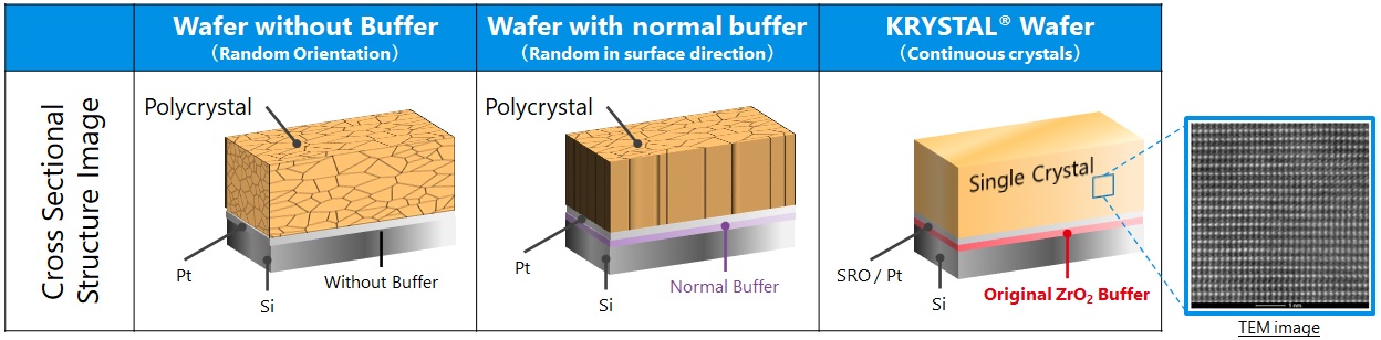
The most distinctive feature of our single crystal technologies is the broad process margin, which is made possible by unique buffer layer technologies.
The buffer layer changes its shape to fill in gaps between the substrate and the crystal lattice of the piezoelectric thin film, creating a single crystal structure with minimal residual stress.
Furthermore, advanced plasma control enables fine-tuning of material characteristics in keeping with the application, with no change in the material composition.
We offer single-crystal piezoelectric thin-film wafers (KRYSTAL® Wafer) for a variety of piezoelectric MEMS applications.
Piezoelectric materials manufactured using basic film structures have the following characteristics:
- They maintain continuous single crystal structures from the silicon (Si) substrate, and reflect single crystal structures without being influenced by the thickness of the piezoelectric thin film
- They have a “ Cube on Cube” structure; that is, a crystal structure somewhat like dice stacked up so they will not roll
- There are few crystal flaws in piezoelectric thin film on strontium ruthenate (SRO), enabling reliable operation even with sub-micron thickness.
These characteristics can be applied not only to PZT (lead zirconate titanate), which is well known as a piezoelectric material, but also to barium titanate (BTO) and numerous other materials as well. Silicon based substrates with a regular (100) orientation are used as a standard, but other orientations have the following characteristics: - When the silicon substrate orientation of <(110) or (111)> is changed, the film orientation can be carried over from the upper layer, providing an optimum combination of materials.
We offer these platforms and proposes ideal combinations to meet the customers’ needs.
Unique Features of KRYSTAL® Wafer's PZT Single-Crystal
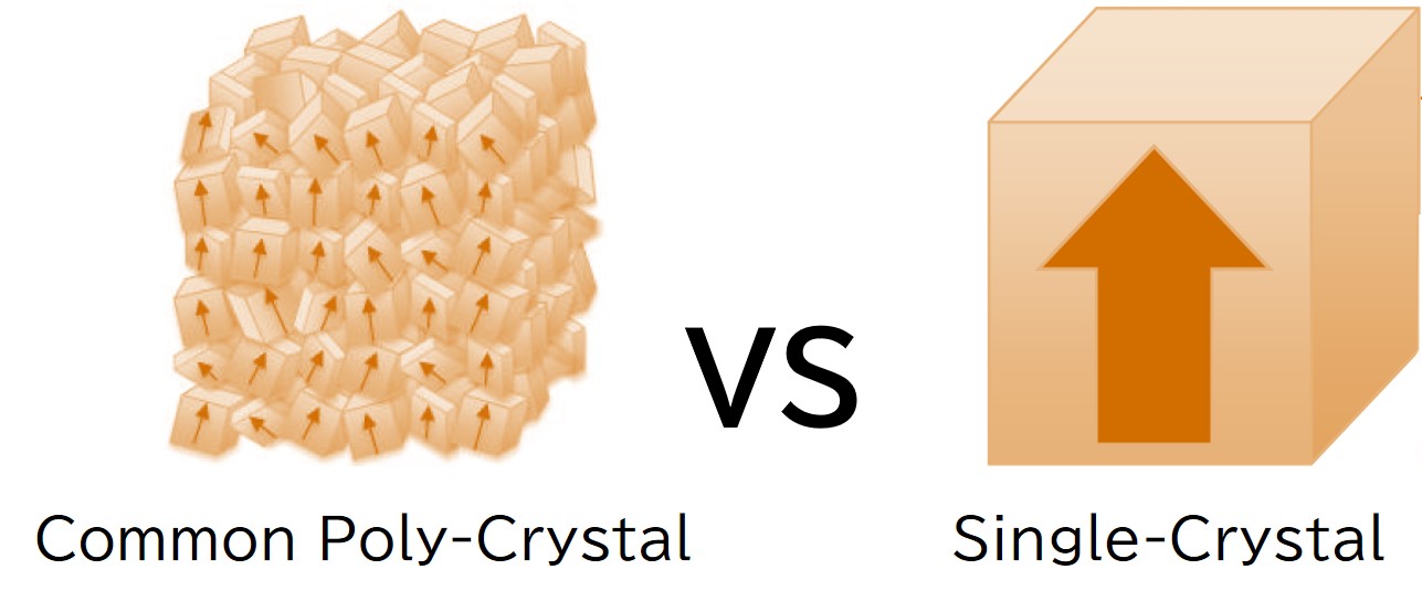
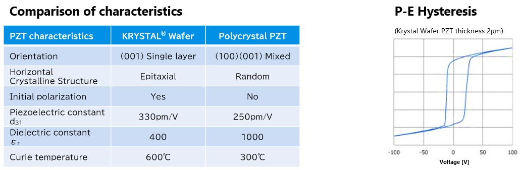
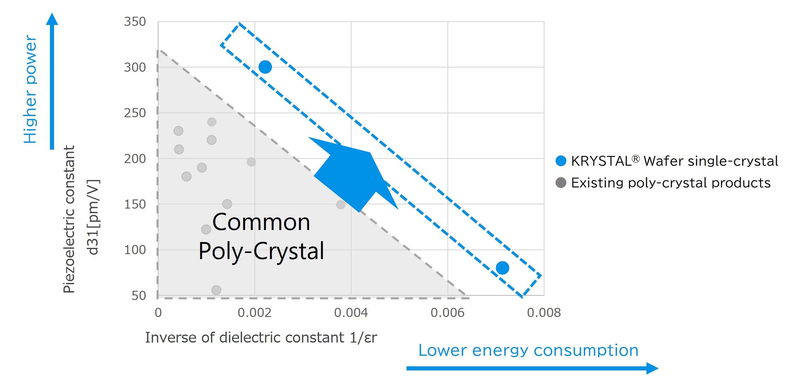
KRYSTAL® Wafer's single-crystal piezoelectric thin films shows superior electrical and mechanical characteristics compared to common poly-crystal piezoelectric thin films.
The most notable features of KRYSTAL® Wafer PZT thin film:
- Single crystal thin film
- Initial polarization from immediately after film forming is maintained
- High heat resistance, with no depolarization even at reflow temperatures (450℃)
- Dielectric constant is less than half compared to polycrystalline materials with similar displacement
-
Superior Electrical and Mechanical Characteristics
The piezoelectric property direction is aligned when single crystalized.
It exhibits superior actuator and sensor performance.
-
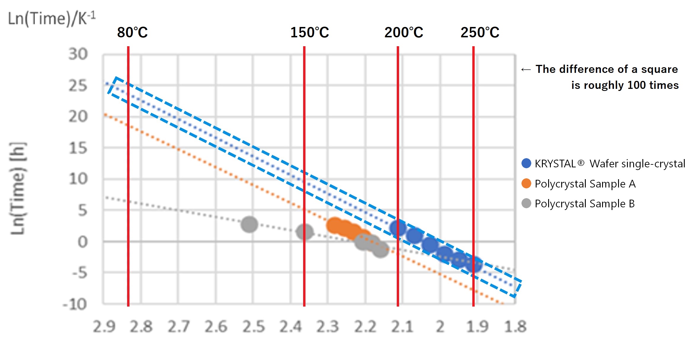
Improved reliability
Single crystallization improves the bonding between atoms.
It has approx. 100 times longer life than polycrystal PZT.
Mechanism of Single-Crystal Deposition by KRYSTAL® Wafer
We have successfully reproduced single-crystallization on customer equipment using KRYSTAL® Wafer.