Mechanism of Single-Crystal Deposition Technologies

There are two types of crystals ‒ single-crystal and polycrystalline ‒ which differ depending on the orientation of grains that make up the crystal.
Single crystal materials are those in which the grains are aligned in a uniform pattern. Diamonds are a perfect example. Diamonds, which are hard and clear, are made of carbon, but so is pencil lead, which is soft and black. The base material is the same, but their characteristics differ dramatically depending on the crystalline state.
Contents:
- Mechanisms of Single-Crystal Thin Film Deposition Technologies
- Single-Crystal PZT Thin Film
- Multi-layer Single-Crystal PZT (2-layer PZT) Thin Film [Under Development]
- Aluminum nitride (AlN) Thin Film [Under development]
Mechanisms of Single-Crystal Thin Film Deposition Technologies
There has been an understanding in the industry that various material characteristics could be improved by adopting single crystal materials, but practical applications have been hindered by engineering difficulties and prohibitive costs. We have overcome these challenges with our proprietary single-crystallization technology and have succeeded in single-crystallizing materials that were previously thought to be impossible.
Along with the production of more products, we are now able to meet a wide range of customer needs.


The key to KRYSTAL® Wafer’s single crystal technologies is in the buffer layer, and the shape of zirconia in particular. A minute pyramid (nano-pyramid) structure grows regularly on the interface surface of platinum or zirconia. This is thought to be because in the case of zirconia, which has a tetragonal structure, the space group has a P4₂/nmc Ditetragonal-dipyramidal structure, so the crystal grows as the pyramid structure is formed. This nano-pyramid structure is the “variable pyramids” depending on the crystal lattice of the piezoelectric material, and it has been proven that structures actually change when different films are formed using different piezoelectric materials. It is possible to automatically control the orientation by changing the upper and lower film in the buffer layer itself, rather than the buffer layer for regular lattice adjustment. In this way, it becomes possible to secure a broad process margin, and to form single crystals using a wide range of materials.
Single-Crystal PZT Thin Film
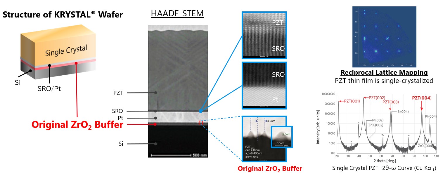
Characteristic data
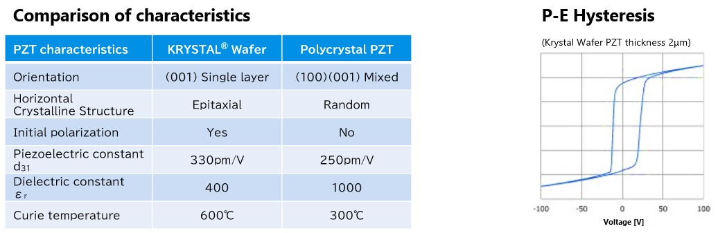
Please note: These data are subject to change due to improvements, etc.
Multi-layer Single-Crystal PZT (2-layer PZT) Thin Film [Under Development]
 We are also developing Multiple layers of single-crystal PZT wafers by applying our superior deposition technology. Piezoelectric properties are improved, enabling high-power and high-precision actuator drive.
Under development with 6 and 8-inch wafers. Please contact us for more details. Contact Us
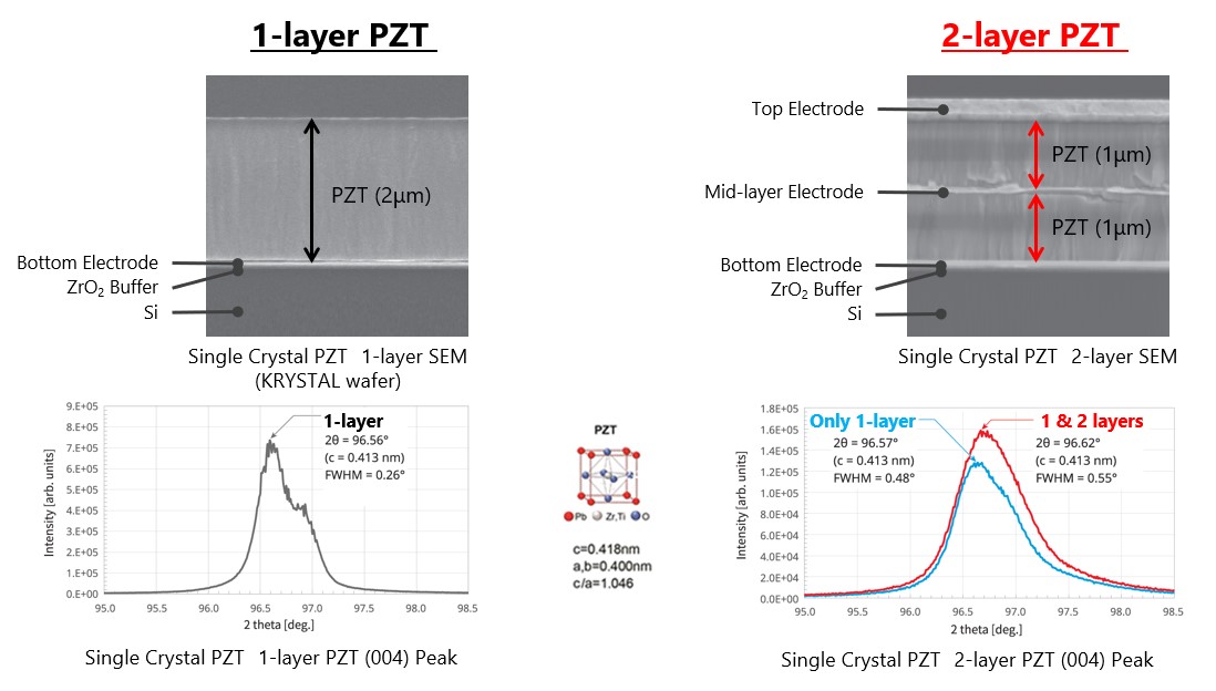
Piezoelectric Properties for 1-layer and 2-layer PZT
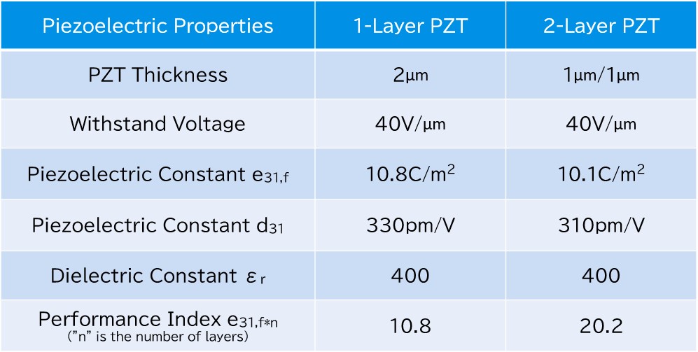
Please note: These data are subject to change due to improvements, etc.
Application example of 2-layer PZT (MEMS Mirror)
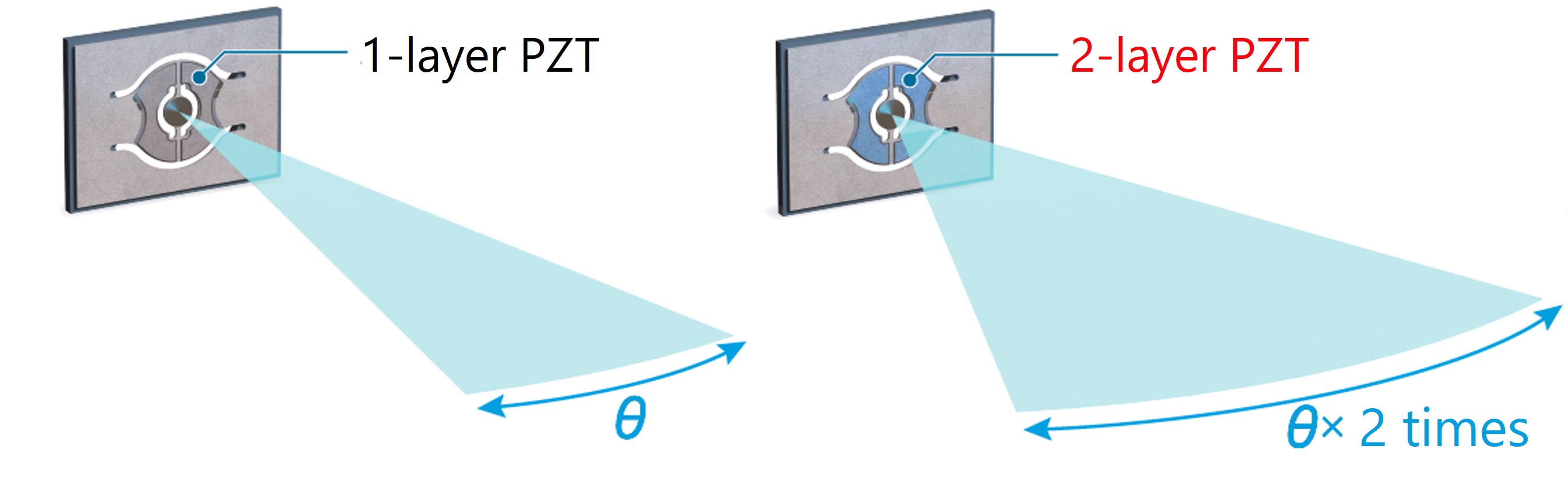
*Simulation example with the same input voltage
Aluminum nitride (AlN) Thin Film [Under development]
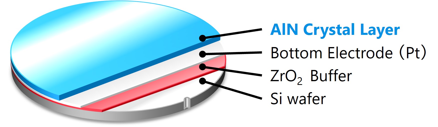 Achieved AlN epitaxial growth on Si wafer using our unique ZrO2 buffer layer technology.
Under development with 6 and 8-inch wafers. Please contact us for more details. Contact Us
Characteristics of AlN Thin Films
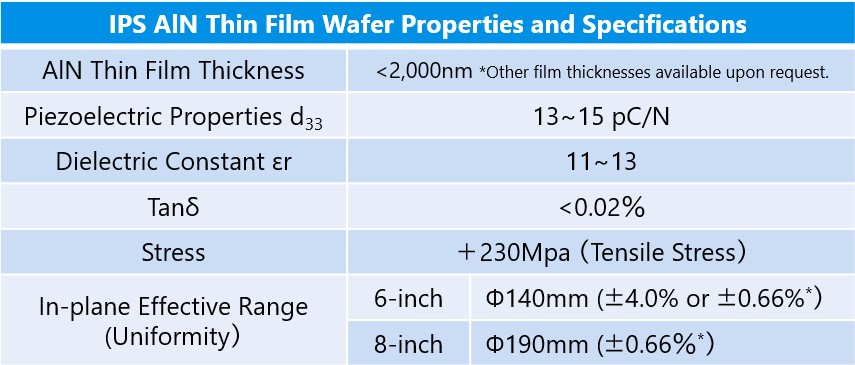
*Uniformity ±0.66% is special product. Please note: These data are subject to change due to improvements, etc.
Measuring Method for Piezoelectric Property d33
Please refer to the documentation for our piezoelectric property d33 measurement method. Download the d33 Measurement Method
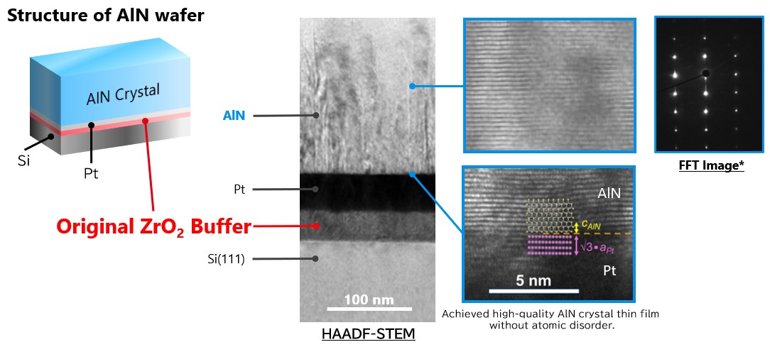
Crystallinity of AlN Thin Films
Confirmed that the lattice constants were aligned and that the AlN crystal thin film was highly oriented and of high quality.
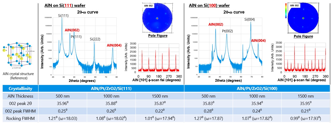
Please note: These data are subject to change due to improvements, etc.