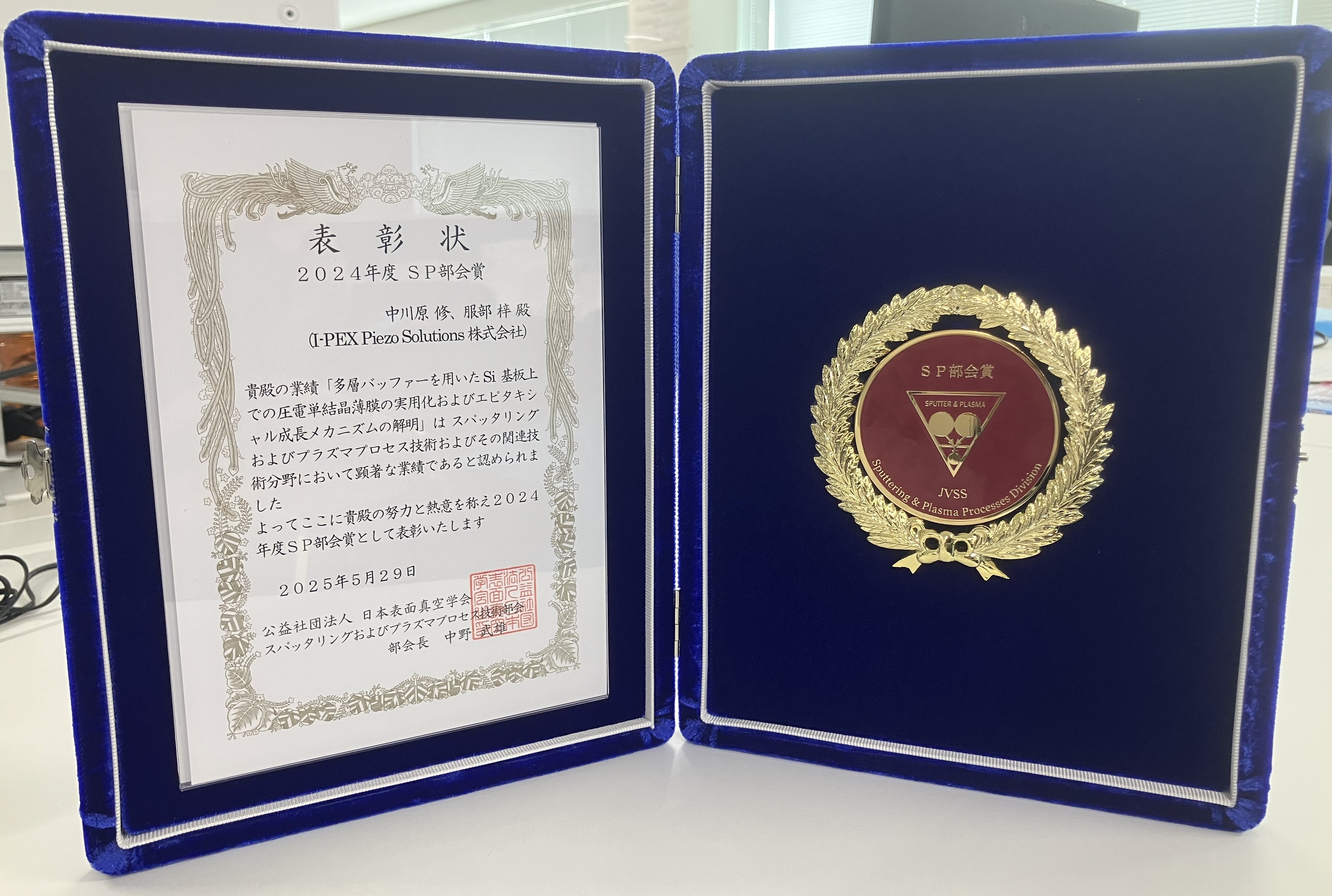
Received the Sputtering and Plasma Process Technology Committee Award
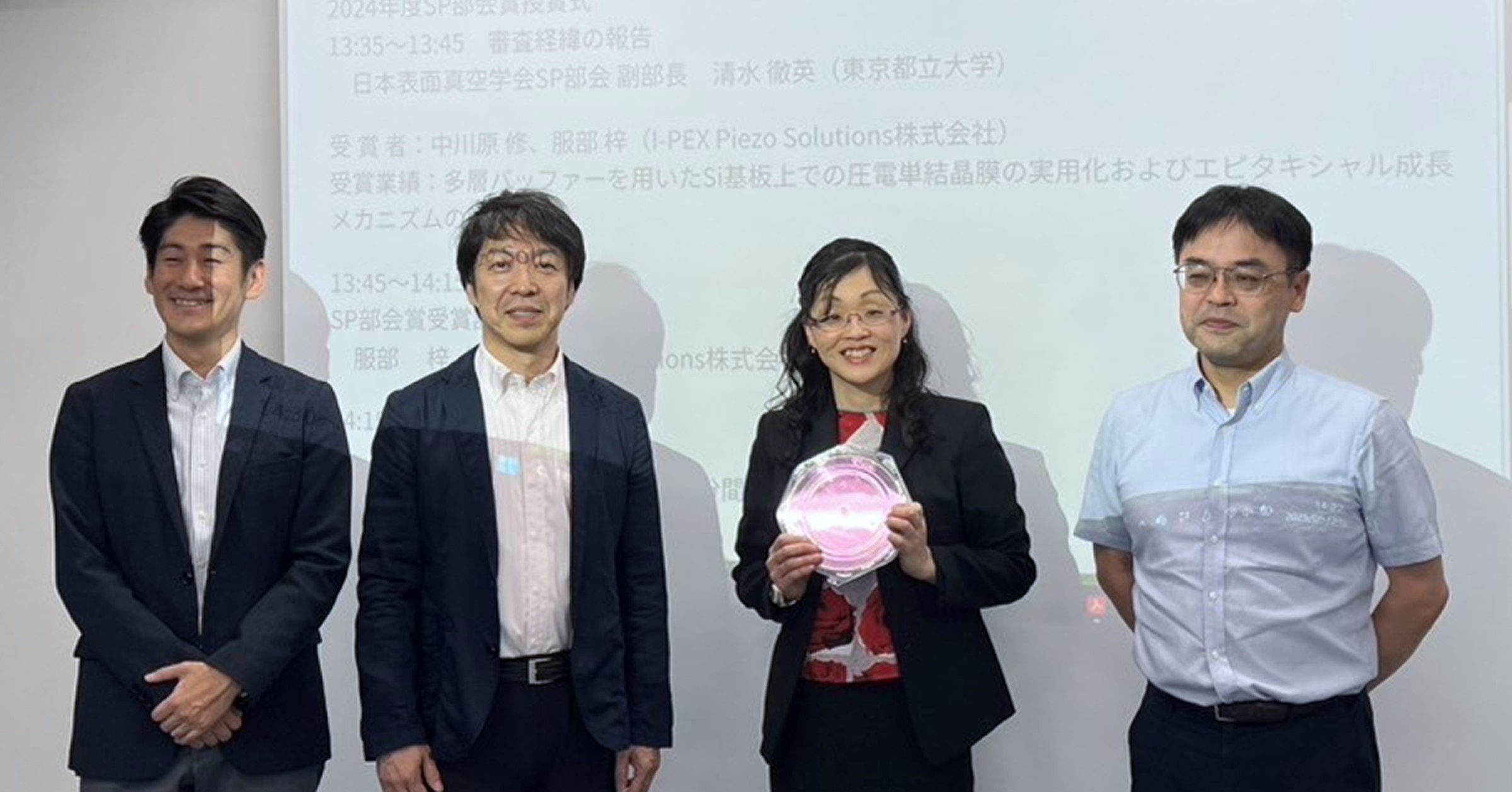
I-PEX Piezo Solutions Inc (hereafter: IPS) has received the “Sputtering and Plasma Process Technology Committee Award 2024” hosted by The Japan Society of Vacuum and Surface Science, which aims to award outstanding achievements that contribute to the development of sputtering and plasma process technology.
Awardees:
Osamu Nakagawara and Azusa Hattori
Achievement:
Practical Application of Piezoelectric Single Crystal Thin Films on Si Substrates with Multilayer Buffers and Elucidation of Epitaxial Growth Mechanism
Reasons for receiving this award
Lead zirconate titanate (PZT), a widely used piezoelectric material, has high piezoelectric properties and is utilized in various MEMS devices such as frequency filters, sensors, transducers, and resonators.
Reference: What is MEMS?
The performance of the PZT piezoelectric thin film is largely dependent on the orientation of the crystals as they are grown. In particular, the effect of piezoelectric thin film performance is strongest when voltage is applied in a direction parallel to or at a certain angle with the direction of PZT polarization.
However, it has not been easy to deposit piezoelectric oxides such as PZT with excellent crystallinity on Si substrates widely used for MEMS because the crystal structures of Si and PZT are not well matched, and the oxide film (SiO₂) that naturally forms on the Si surface and the diffusion of elements at the interface are factors that inhibit growth.
IPS has developed a proprietary multilayer buffer layer technology that enables the deposition of single-crystal PZT thin films on large-area Si substrates (6“ and 8”) while maintaining atomic-level uniformity. This technology, which simultaneously satisfies the requirements of in-plane crystallographic orientation, interface structure control, and thin film homogeneity, is the result of a combination of advanced technological capabilities in multiple areas, including optimization of deposition conditions, precise equipment control, and material design.
Reference: Mechanism of single crystallization by IPS film deposition technology
The award was given in recognition of the detailed analysis of the structural changes that occur at the boundaries of these multilayer buffer layers using atomic-level observation techniques, and the clarification of the mechanism of continuously connected multilayer hetero-epitaxial growth and boundary formation.
This knowledge has enabled a new approach to bonding different materials and layering materials with different functionality, which were previously considered difficult to achieve, and is expected to make a significant contribution as a fundamental technology in the development of high-performance and highly functional devices and the creation of new materials in the future.