全球領先的壓電技術

通過DLC成膜的等離子控制技術與無機晶體控制技術相結合,我們成功地將被認為極難合成的壓電材料單晶化, 並建立了製造方法。單晶技術能夠應用在各種半導體加工,同時表現出比現有多晶材料更高的性能。
內容:
單晶薄膜的特色
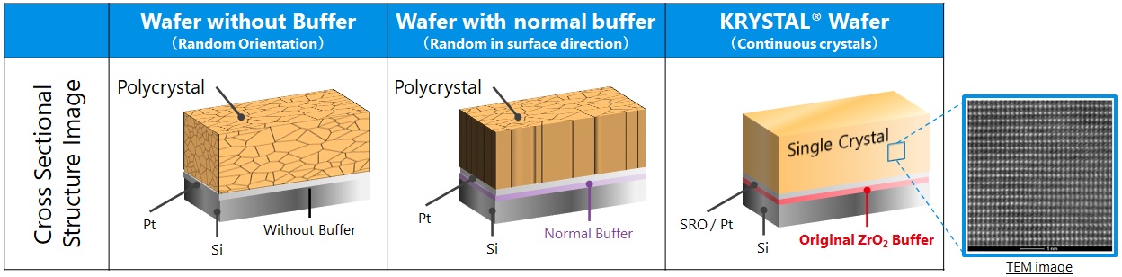
我們的單晶技術最顯著的特點就是寬廣的製程邊隙,這是由獨特的緩衝層技術所實現的。
緩衝層可改變形狀,填補基板與壓電薄膜晶格之間的空隙,形成殘留應力最小的單晶結構。
此外,先進的等離子控制可根據應用微調材料特性,而不改變材料成分。
我們提供單晶壓電薄膜晶圓 (KRYSTAL® Wafer),適用於各種壓電 MEMS 應用。
使用基本薄膜結構製造的壓電材料具有以下特性:
- They maintain continuous single crystal structures from the silicon (Si) substrate, and reflect single crystal structures without being influenced by the thickness of the piezoelectric thin film
- They have a “ Cube on Cube” structure; that is, a crystal structure somewhat like dice stacked up so they will not roll
- There are few crystal flaws in piezoelectric thin film on strontium ruthenate (SRO), enabling reliable operation even with sub-micron thickness.
These characteristics can be applied not only to PZT (lead zirconate titanate), which is well known as a piezoelectric material, but also to barium titanate (BTO) and numerous other materials as well. Silicon based substrates with a regular (100) orientation are used as a standard, but other orientations have the following characteristics: - When the silicon substrate orientation of <(110) or (111)> is changed, the film orientation can be carried over from the upper layer, providing an optimum combination of materials.
我們提供這些平台,並建議理想的組合,以滿足客戶的需求。
KRYSTAL® Wafer 的 PZT 單晶獨特之處
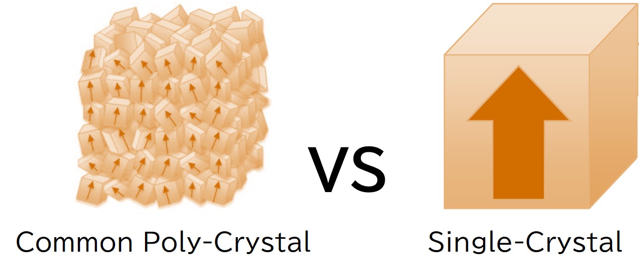
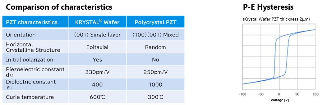
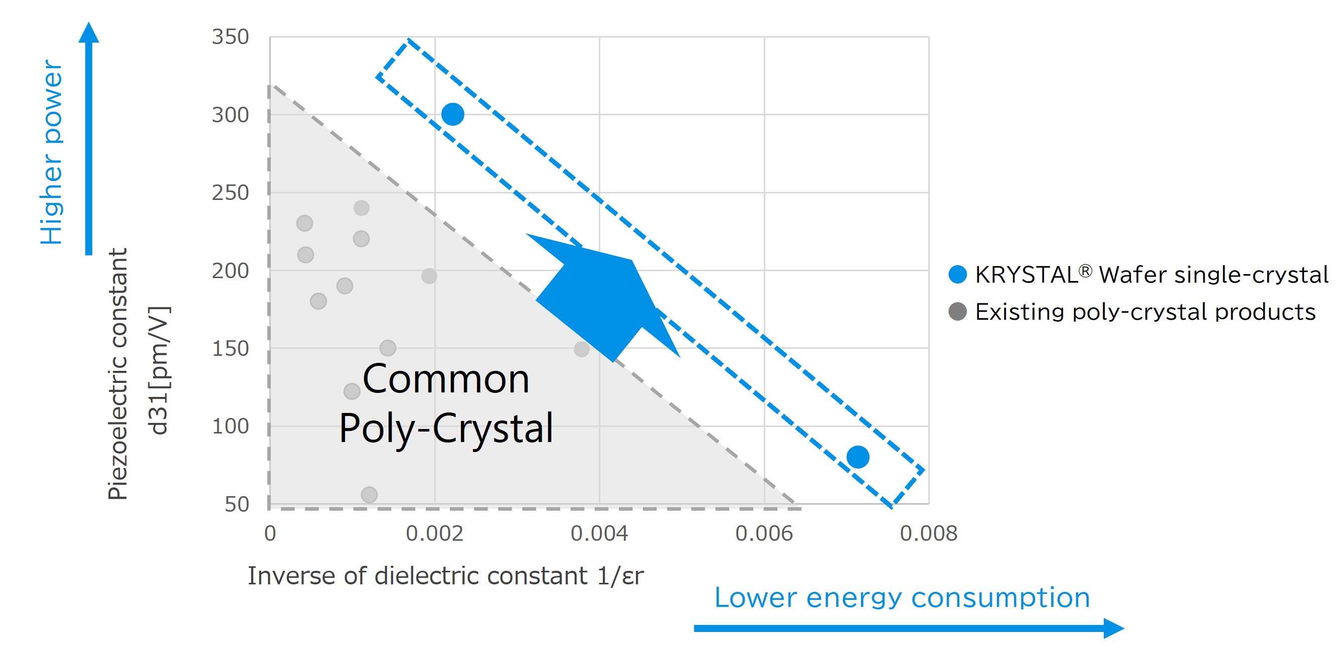
KRYSTAL® Wafer 的單晶壓電薄膜與一般多晶壓電薄膜相比,具有更優異的電氣與機械特性。
KRYSTAL® Wafer PZT 薄膜最顯著的特點:
- 單晶薄膜
- 可維持成膜後的初始極化
- 耐熱性高,即使在回流溫度 (450℃) 下也不會產生去極化現象
- 介電常數小於具有類似位移的多晶材料的一半
-
優異的電氣與機械特性
壓電特性方向在單晶化時是對齊的。
它展現出優異的致動器和傳感器性能。
-
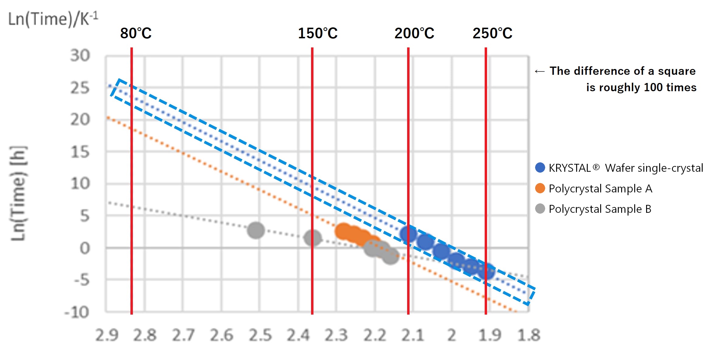
提高可靠性
單結晶改善了原子之間的結合。
它的壽命比多晶體 PZT 長約 100 倍。
KRYSTAL® Wafer 的單晶沉積機制
我們已使用 KRYSTAL® Wafer 在客戶設備上成功重製單結晶。